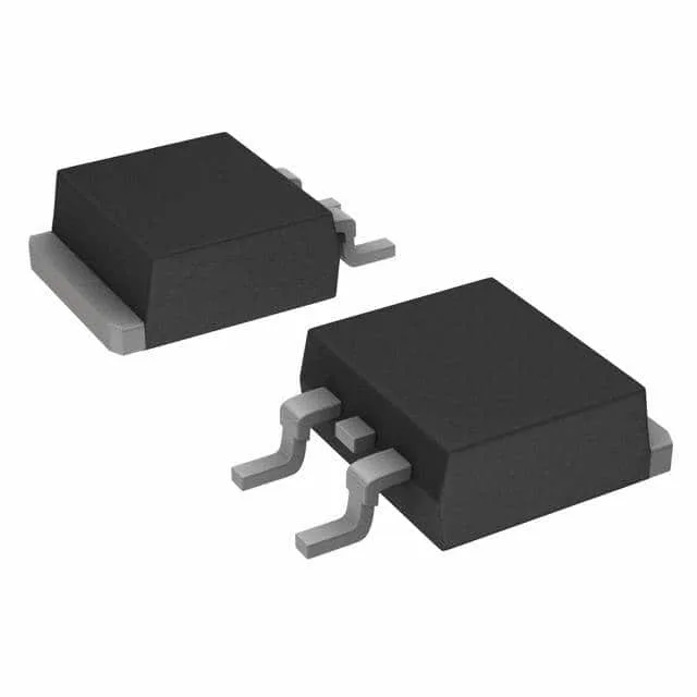
Infineon Technologies IDK05G120C5XTMA1

IDK05G120C5XTMA1 Infineon CoolSiC™+ SiC Schottky Diode

MPNIDK05G120C5XTMA1
End of Life

Infineon CoolSiC™+ IDK05G120C5XTMA1, Silicon Carbide Schottky Diode, 1200 V DC reverse, 19.1 A average rectified, No Recovery Time > 500 mA, -55°C to 175°C junction, PG-TO263-2-1 surface mount.

$4.24Ref. price · indicative, final on quote
PackagingTO-263-3, D²Pak (2 Leads + Tab), TO-263AB
StockContact for availability
MOQ1 pcs
  • 100% new & originalTraceable channels only — no refurbs, no pulls, no remarked parts.
  • Date & lot codes on quoteStated per line before you commit; label photos on request.
  • MSL-compliant ESD packingMoisture-sealed bags with indicator cards; reels photo-verified.
  • PayPal buyer protectionPay by T/T, PayPal or Payoneer — card payments covered end to end.

Specifications

IDK05G120C5XTMA1 Technical Specifications
ParameterValue
SeriesCoolSiC™+
Diode typeSilicon Carbide Schottky
Mounting typeSurface Mount
Voltage - DC reverse (Vr)1200 V
Voltage - forward (Vf) (Max) @ if1.8 V @ 5 A
Current - reverse leakage @ vr33 µA @ 1200 V
Current - average rectified19.1A
Operating temperature - junction-55°C ~ 175°C
SpeedNo Recovery Time > 500mA (Io)
PackageTape & Reel (TR); Cut Tape (CT)
CaseTO-263-3, D²Pak (2 Leads + Tab), TO-263AB
Capacitance @ vr, f301pF @ 1V, 1MHz

Product details

1.2 kV SiC Schottky with zero reverse-recovery — the switching-loss killer

The IDK05G120C5XTMA1 is Infineon's CoolSiC™+ generation silicon carbide Schottky diode, rated for a 1200 V DC reverse voltage and 19.1 A average rectified forward current. The headline spec that makes this part a drop-in upgrade over a fast-recovery silicon diode is the zero reverse-recovery charge — listed as No Recovery Time > 500 mA — which means the diode does not store minority carriers. In a hard-switched PFC or inverter leg, that eliminates the reverse-recovery current spike that costs switching loss and rings up EMI in a Si FRED.

Forward drop and junction temperature — the thermal budget

Forward voltage is specified at 1.8 V maximum at 5 A forward current. That is the conduction loss reference for a typical operating point — at 19.1 A the Vf will be higher, but the 5 A point is where most continuous-load designs will size their average current. The junction temperature range runs from -55°C to 175°C, which is the full SiC temperature envelope. The 175°C maximum allows the die to run hotter than a 150°C Si junction, which buys margin in a tightly packed power stage where the ambient around the diode is elevated by nearby magnetics and MOSFETs.

Package and mounting — the TO-263 footprint

The part ships in a TO-263-3 (D²Pak) surface-mount package, supplier device code PG-TO263-2-1. This is a standard D²Pak footprint with a large exposed tab on the back side — the tab is the cathode connection and the primary thermal path. The board layout must provide a copper pad and thermal vias under the tab to pull heat into the inner-layer planes. The package is supplied on Tape & Reel or Cut Tape, which suits both reflow assembly and prototype hand-placing.

Lifecycle and compliance

It is listed as ROHS3 compliant, so no exemption-based restrictions on lead or other substances.

Frequently asked questions

Is IDK05G120C5XTMA1 RoHS compliant?

Yes — the part is listed as ROHS3 Compliant.

What does No Recovery Time > 500 mA mean for my design?

It means the SiC Schottky has essentially zero reverse-recovery charge. Unlike a silicon fast-recovery diode, there is no stored minority charge to sweep out when the diode commutates — so the reverse-recovery current spike and the associated switching loss are eliminated. This is the primary reason to select a SiC Schottky over a Si FRED in a hard-switched topology like a continuous-conduction-mode PFC or a phase-leg inverter.