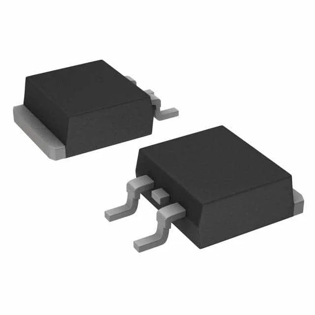
Infineon Technologies IDK04G65C5XTMA2

Infineon IDK04G65C5XTMA2 SiC Schottky Diode, 650V 4A D²Pak

MPNIDK04G65C5XTMA2
End of Life

Infineon CoolSiC™+ IDK04G65C5XTMA2 SiC Schottky diode, 650 V reverse voltage, 4 A average rectified current, 0 ns reverse recovery time, -55°C to 175°C junction temperature, surface-mount D²Pak (TO-263-2) package.

$2.18Ref. price · indicative, final on quote
PackagingTO-263-3, D²Pak (2 Leads + Tab), TO-263AB
StockContact for availability
MOQ1 pcs
  • 100% new & originalTraceable channels only — no refurbs, no pulls, no remarked parts.
  • Date & lot codes on quoteStated per line before you commit; label photos on request.
  • MSL-compliant ESD packingMoisture-sealed bags with indicator cards; reels photo-verified.
  • PayPal buyer protectionPay by T/T, PayPal or Payoneer — card payments covered end to end.

Specifications

IDK04G65C5XTMA2 Technical Specifications
ParameterValue
SeriesCoolSiC™+
Mounting typeSurface Mount
Voltage - DC reverse (Vr)650 V
Voltage - forward (Vf) (Max) @ if1.8 V @ 4 A
Current - reverse leakage @ vr670 µA @ 650 V
Current - average rectified4A
Operating temperature - junction-55°C ~ 175°C
SpeedNo Recovery Time > 500mA (Io)
PackageTape & Reel (TR); Cut Tape (CT)
TechnologySiC (Silicon Carbide) Schottky
CaseTO-263-3, D²Pak (2 Leads + Tab), TO-263AB
Capacitance @ vr, f130pF @ 1V, 1MHz
Reverse recovery time0 ns

Product details

What this SiC Schottky brings to the power stage

The Infineon IDK04G65C5XTMA2 is a 650 V, 4 A silicon-carbide Schottky diode from the CoolSiC™+ generation, built for hard-switched power converters where silicon ultrafast diodes leave switching losses on the table. Its zero reverse-recovery time (0 ns trr) means the diode never stores minority carriers — no recovery charge to sweep out, no dead-time penalty in a continuous-conduction-mode PFC boost stage or a phase-shifted full bridge. The 175 °C maximum junction temperature gives headroom for high-ambient telecom rectifiers and solar inverters where the thermal loop is tight.

Package and thermal path

The D²Pak (TO-263-2) surface-mount package puts the die close to the PCB copper pour — the tab is the cathode terminal and the primary heat path. Layout needs sufficient copper area on the drain pad to keep the junction below 175 °C at full load.

Lifecycle and sourcing posture

The IDK04G65C5XTMA2 carries an Active product status — no last-time-buy notice, no NRND flag. Infineon continues to manufacture the CoolSiC™+ generation alongside the newer Gen6 and G7 families, so this part remains a valid selection for production builds.

Frequently asked questions

Can I use IDK04G65C5XTMA2 in a PFC circuit?

Yes. The 650 V blocking voltage and 0 ns reverse recovery time make it well suited for continuous-conduction-mode PFC boost stages operating from a 400 VDC bus. The 4 A average rating fits 1 kW-class single-phase designs with adequate heatsinking.