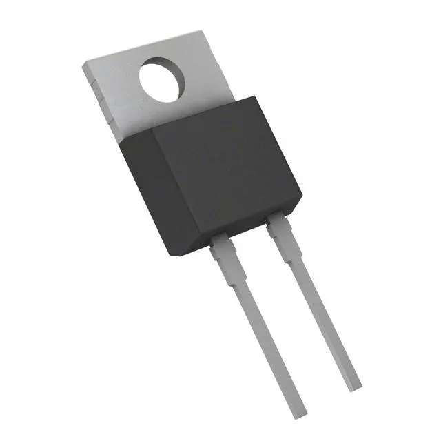
Infineon Technologies IDH20G65C6XKSA1

IDH20G65C6XKSA1 SiC Schottky Diode, 650 V, 41 A, TO-220-2

MPNIDH20G65C6XKSA1
End of Life

Infineon CoolSiC IDH20G65C6XKSA1, Silicon Carbide Schottky Diode, 650 V reverse, 41 A average rectified, 0 ns reverse recovery, TO-220-2 through-hole, -55 to 175 °C junction.

$7.66Ref. price · indicative, final on quote
PackagingTO-220-2
StockContact for availability
MOQ1 pcs
  • 100% new & originalTraceable channels only — no refurbs, no pulls, no remarked parts.
  • Date & lot codes on quoteStated per line before you commit; label photos on request.
  • MSL-compliant ESD packingMoisture-sealed bags with indicator cards; reels photo-verified.
  • PayPal buyer protectionPay by T/T, PayPal or Payoneer — card payments covered end to end.

Specifications

IDH20G65C6XKSA1 Technical Specifications
ParameterValue
Mounting typeThrough Hole
Voltage - DC reverse (Vr)650 V
Voltage - forward (Vf) (Max) @ if1.35 V @ 20 A
Current - reverse leakage @ vr67 µA @ 420 V
Current - average rectified41A
Operating temperature - junction-55°C ~ 175°C
SpeedNo Recovery Time > 500mA (Io)
PackageTube
TechnologySiC (Silicon Carbide) Schottky
CaseTO-220-2
Capacitance @ vr, f970pF @ 1V, 1MHz
Reverse recovery time0 ns

Product details

SiC Schottky with zero recovery — the switching-loss killer

The Infineon IDH20G65C6XKSA1 is a 650 V, 41 A Silicon Carbide Schottky diode in a TO-220-2 through-hole package. Its defining characteristic is zero reverse recovery time (0 ns trr) — no stored charge to sweep out, which means the switching loss in a hard-switched converter is limited to the junction capacitance alone, not a Qrr tail.

650 V blocking, 41 A forward — where it fits

With a 650 V DC reverse voltage rating and 41 A average rectified current, this diode is sized for the output stage of a 400 V bus PFC boost converter or the secondary side of a high-voltage DC-DC stage. The 1.35 V forward voltage at 20 A (Vf max) is typical for a SiC Schottky of this current class — the conduction loss is higher than a comparable ultrafast silicon diode, but the switching loss saving more than compensates above 50 kHz. The 67 µA reverse leakage at 420 V and 970 pF capacitance at 1 V are the two parameters that set the no-load dissipation and the capacitive switching loss respectively. At light load the leakage dominates; at full load the Vf × If product sets the junction temperature.

175 °C junction — no derating compromise

The wide temperature range means the same BOM can be qualified across industrial and automotive programs without a second temperature-grade variant.

ROHS3 compliant.

Frequently asked questions

What is the reverse recovery time of IDH20G65C6XKSA1?

Zero nanoseconds — the SiC Schottky structure has no minority carrier storage, so trr is effectively 0 ns. This eliminates the reverse recovery loss that plagues ultrafast silicon diodes in hard-switched topologies.

Is IDH20G65C6XKSA1 RoHS compliant?

Yes, it is ROHS3 compliant — meets the current EU RoHS exemption rules with no restricted substances above threshold.