What the zero reverse recovery time means for the switching stage
The Infineon IDDD12G65C6XTMA1 is a CoolSiC™+ Silicon Carbide Schottky diode rated for 650 V reverse voltage and 34 A average rectified current. In a hard-switched PFC boost or inverter leg, that eliminates the reverse-recovery loss spike that a silicon ultrafast diode would generate, which directly reduces the switching loss in the companion MOSFET or IGBT and lowers the overall junction temperature in the power stage.
Package and mounting — what fits the board
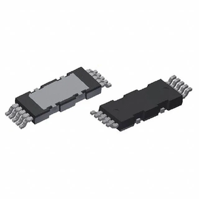
The part is supplied in a 10-PowerSOP Module (PG-HDSOP-10-1), a surface-mount package designed for automated assembly. The 594 pF capacitance at 1 V, 1 MHz is the small-signal value; in a switching application the effective output capacitance is lower under reverse bias, so the driver sees a manageable capacitive turn-on current.
Infineon lists the IDDD12G65C6XTMA1 as an active product with ROHS3 compliance.