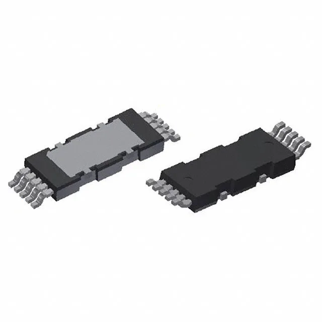
Infineon Technologies IDDD10G65C6XTMA1

Infineon IDDD10G65C6XTMA1 SiC Schottky Diode, 650 V 29 A

MPNIDDD10G65C6XTMA1
End of Life

Infineon CoolSiC™+ IDDD10G65C6XTMA1, Silicon Carbide Schottky Diode, 650 V DC Reverse, 29 A Average Rectified, No Recovery Time >500 mA, PG-HDSOP-10-1 Package, Surface Mount, -55 to 175 °C Junction.

$5.12Ref. price · indicative, final on quote
Packaging10-PowerSOP Module
StockContact for availability
MOQ1 pcs
  • 100% new & originalTraceable channels only — no refurbs, no pulls, no remarked parts.
  • Date & lot codes on quoteStated per line before you commit; label photos on request.
  • MSL-compliant ESD packingMoisture-sealed bags with indicator cards; reels photo-verified.
  • PayPal buyer protectionPay by T/T, PayPal or Payoneer — card payments covered end to end.

Specifications

IDDD10G65C6XTMA1 Technical Specifications
ParameterValue
SeriesCoolSiC™+
Diode typeSilicon Carbide Schottky
Mounting typeSurface Mount
Voltage - DC reverse (Vr)650 V
Current - reverse leakage @ vr33 µA @ 420 V
Current - average rectified29A
Operating temperature - junction-55°C ~ 175°C
SpeedNo Recovery Time > 500mA (Io)
PackageTape & Reel (TR); Cut Tape (CT)
Case10-PowerSOP Module
Capacitance @ vr, f495pF @ 1V, 1MHz
Reverse recovery time0 ns

Product details

Zero-recovery switching — what it buys the power stage

The IDDD10G65C6XTMA1 is a silicon carbide Schottky diode from Infineon's CoolSiC+ generation. Its defining characteristic is zero reverse recovery time — the datasheet lists No Recovery Time > 500 mA (Io), which means the diode turns off with virtually no stored charge to sweep out. In a hard-switched PFC or inverter leg, that eliminates the reverse-recovery loss spike that plagues ultrafast silicon diodes, keeping the MOSFET or IGBT switch cooler and allowing higher switching frequencies without a thermal penalty.

650 V / 29 A — headroom for 400 VDC bus designs

Rated 650 V DC reverse and 29 A average rectified forward current, this diode comfortably covers the 400 VDC bus common in three-phase industrial drives, EV on-board chargers, and server PFC stages. The 650 V rating provides derating margin above the nominal bus voltage; the 29 A average current supports several kilowatts of output in a boost or bridgeless PFC topology. Junction temperature range extends from -55 °C to 175 °C, so the diode can sit in a hot enclosure or near a heatsink without forced air and still deliver its rated current.

PG-HDSOP-10-1 — surface-mount power package

Housed in a PG-HDSOP-10-1 module — Infineon's 10-lead surface-mount power package — the diode's large solderable pads carry the thermal path to the PCB copper plane. The package is a 10-PowerSOP module, surface-mount only, so the board layout must allocate enough copper area on the drain tab to keep junction temperature within the 175 °C limit at full load. No through-hole mounting; reflow profile follows standard lead-free solder (ROHS3 compliant).

Infineon lists this part with an Active product status. ROHS3 compliant, so it passes into EU and regional markets without an exemption expiry.

Frequently asked questions

Where can I buy IDDD10G65C6XTMA1?

Sourcing buyers need to find authorized distributors quickly to avoid counterfeit and secure best pricing.

What are the key specifications of IDDD10G65C6XTMA1?

Design engineers must verify electrical and thermal specs (650V, 29A, 0ns trr) to confirm fit in their application.

Is IDDD10G65C6XTMA1 RoHS compliant?

Compliance status is critical for regulatory and environmental requirements; buyers often filter by RoHS.

What is the lead time for IDDD10G65C6XTMA1?

Lead time affects production schedules; sourcing buyers need this to plan procurement.

Can IDDD10G65C6XTMA1 be used as a replacement for IDDD10G65C6?

Maintenance techs and brokers often seek cross-references when substituting or checking lifecycle.

What is the package type of IDDD10G65C6XTMA1?

Mechanical fit is essential for both design and replacement; HDSOP-10 footprint must match PCB or existing socket.