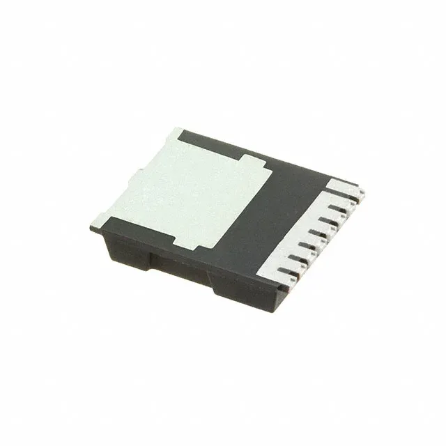
Infineon Technologies IAUT300N08S5N011ATMA1

Infineon IAUT300N08S5N011ATMA1 N-Channel MOSFET, 80 V

MPNIAUT300N08S5N011ATMA1
End of Life

Infineon OptiMOS™ IAUT300N08S5N011ATMA1, N-channel MOSFET, 80 V drain-source, 410 A continuous drain, 1.1 mOhm Rds(on) at 100 A, PG-HSOF-8-1 package, -55°C to 175°C junction temperature.

$5.6Ref. price · indicative, final on quote
Packaging8-PowerSFN
StockContact for availability
MOQ1 pcs
  • 100% new & originalTraceable channels only — no refurbs, no pulls, no remarked parts.
  • Date & lot codes on quoteStated per line before you commit; label photos on request.
  • MSL-compliant ESD packingMoisture-sealed bags with indicator cards; reels photo-verified.
  • PayPal buyer protectionPay by T/T, PayPal or Payoneer — card payments covered end to end.

Specifications

IAUT300N08S5N011ATMA1 Technical Specifications
ParameterValue
SeriesOptiMOS™
FET typeN-Channel
Mounting typeSurface Mount
Drain to source voltage80 V
Drive voltage (Max rds on, min rds on)6V, 10V
Current - continuous drain (Id) @ 25°C410A (Tj)
Power dissipation375W (Tc)
Operating temperature-55°C ~ 175°C (TJ)
PackageTape & Reel (TR); Cut Tape (CT)
Vgs±20V
TechnologyMOSFET (Metal Oxide)
Case8-PowerSFN
Vgs(th) (Max) @ id3.8V @ 275µA
Rds on (Max) @ id, vgs1.1mOhm @ 100A, 10V
Gate charge (Qg) (Max) @ vgs231 nC @ 10 V
Input capacitance (Ciss) (Max) @ vds16250 pF @ 40 V

Product details

80 V, 1.1 mOhm — conduction loss floor for high-current switching

The 1.1 mOhm figure is the value the designer uses for worst-case dissipation at full load; actual Rds(on) rises with junction temperature per the normalised curve in the datasheet.

Gate charge and drive budget

Total gate charge Qg is 231 nC at 10 V. For a 100 kHz switching frequency, the gate driver must supply an average current of about 23 mA, but the peak current during the Miller plateau is what determines switching speed. The 16250 pF input capacitance at 40 V drain-source confirms this is a large-die device — the driver output stage needs enough peak current to charge and discharge that capacitance within the dead-time budget. The recommended drive voltage range is 6 V to 10 V for achieving the rated Rds(on). Using 6 V gate drive increases on-resistance above the 1.1 mOhm figure; the 10 V drive is the standard for reaching the minimum Rds(on) stated in the datasheet.

Package and thermal path

The PG-HSOF-8-1 package (8-PowerSFN) is a surface-mount power package with an exposed drain pad on the bottom. The 375 W maximum power dissipation at case temperature assumes the pad is soldered to a sufficient copper area on the PCB — the thermal resistance from junction to case is the limiting factor, not the silicon itself.

Lifecycle and compliance

The ±20 V maximum gate-source voltage is standard for this voltage class and compatible with most gate drivers.

Frequently asked questions

Is IAUT300N08S5N011ATMA1 RoHS compliant?

Yes, it is ROHS3 compliant.