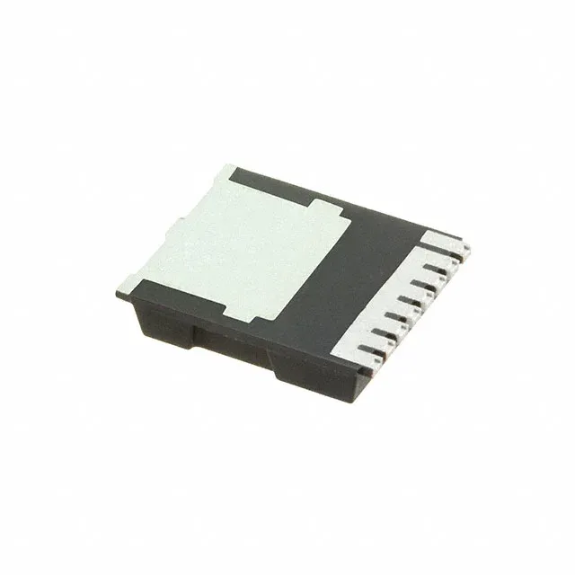
Infineon Technologies IAUT260N10S5N019ATMA1

IAUT260N10S5N019ATMA1 OptiMOS-5 N-Ch 100V 260A PG-HSOF-8-1

MPNIAUT260N10S5N019ATMA1
End of Life

Infineon OptiMOS™-5, N-Channel MOSFET, IAUT260N10S5N019ATMA1, 100 V, 260 A, 1.9 mOhm Rds(on) @ 10 V, PG-HSOF-8-1, -55°C to 175°C.

$5.14Ref. price · indicative, final on quote
Packaging8-PowerSFN
StockContact for availability
MOQ1 pcs
  • 100% new & originalTraceable channels only — no refurbs, no pulls, no remarked parts.
  • Date & lot codes on quoteStated per line before you commit; label photos on request.
  • MSL-compliant ESD packingMoisture-sealed bags with indicator cards; reels photo-verified.
  • PayPal buyer protectionPay by T/T, PayPal or Payoneer — card payments covered end to end.

Specifications

IAUT260N10S5N019ATMA1 Technical Specifications
ParameterValue
SeriesOptiMOS™-5
FET typeN-Channel
Mounting typeSurface Mount
Drain to source voltage100 V
Drive voltage (Max rds on, min rds on)6V, 10V
Current - continuous drain (Id) @ 25°C260A (Tc)
Power dissipation300W (Tc)
Operating temperature-55°C ~ 175°C (TJ)
PackageTape & Reel (TR); Cut Tape (CT)
Vgs±20V
TechnologyMOSFET (Metal Oxide)
Case8-PowerSFN
Vgs(th) (Max) @ id3.8V @ 210µA
Rds on (Max) @ id, vgs1.9mOhm @ 100A, 10V
Gate charge (Qg) (Max) @ vgs166 nC @ 10 V
Input capacitance (Ciss) (Max) @ vds11830 pF @ 50 V

Product details

100 V, 260 A switching — the 1.9 mOhm floor

The IAUT260N10S5N019ATMA1: The drive voltage window (6 V to 10 V) means it can be driven from a 10 V rail for minimum Rds(on) or from a 6 V rail if the gate-driver supply is lower, though the 10 V figure is the one to design around for full performance.

Package and thermal — PG-HSOF-8-1

Housed in the 8-lead PowerSFN (PG-HSOF-8-1) surface-mount package, this part relies on the exposed pad for heat sinking. The 8-PowerSFN footprint is smaller than a D2PAK but demands a multi-layer board with adequate copper pour for 260 A continuous current; the PCB trace width and via count must be sized for the load, not just the package rating.

Gate charge and switching speed

Total gate charge (Qg) is 166 nC at 10 V, and input capacitance (Ciss) is 11830 pF at 50 V drain-source. These numbers tell the gate-driver designer how much current is needed to switch the FET at the target frequency: a 1 A gate driver can charge 166 nC in about 166 ns, but the Miller plateau and the 11830 pF Ciss will shape the actual rise/fall times. For a 100 kHz hard-switching converter, the gate-drive losses alone (Qg × Vgs × fsw) add up — budget around 0.17 W per FET at 100 kHz, which is manageable but not negligible.

Temperature grade and environment

The 175°C ceiling is above the typical 150°C limit for many 100 V MOSFETs, which makes this part suited for under-hood automotive, industrial motor drives with high ambient temperature, or any environment where junction temperature spikes during overload. The threshold voltage (Vgs(th)) is 3.8 V maximum at 210 µA drain current, so the gate drive must swing well above 3.8 V to fully enhance the channel — the 6 V minimum drive voltage in the spec is the practical floor.

Frequently asked questions

What is the RDS(on) of IAUT260N10S5N019ATMA1?

This is the figure to use for worst-case conduction loss calculations in your power stage.

Is IAUT260N10S5N019ATMA1 lead-free and RoHS compliant?

Yes, the part carries ROHS3 compliance status, meaning it meets the latest RoHS directive including the exemption for lead in high-melting-temperature solders.