With a maximum Rds(on) of 7.3 mOhm at 30 A and 10 V, conduction losses stay low even at high current. The gate charge is 22.6 nC at 10 V, which means the driver doesn't need to push a large charge into the gate for each switching cycle — a benefit for moderate-frequency PWM applications like motor drives or DC-DC converters. The drive voltage threshold is 2.2 V at 19 µA, so the part can be turned on with logic-level gate signals (4.5 V is the minimum recommended drive for the rated Rds(on)), but the 10 V drive delivers the lowest on-resistance.
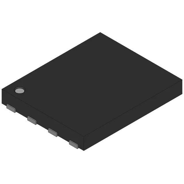
Package and mounting — PG-TDSON-8-33
The supplier device package is PG-TDSON-8-33; the standard package / case is 8-PowerTDFN. Surface-mount assembly requires a solder paste stencil designed for the large thermal pad to ensure adequate solder joint coverage and heat transfer.