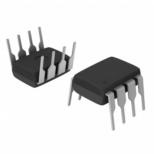
The Cypress (now Infineon) FM25V20-PG is a 2Mbit non-volatile ferroelectric RAM (FRAM) organized as 256K x 8 bits, accessed over an SPI bus at up to 40 MHz. FRAM combines the fast write speed and low power of SRAM with the non-volatility of Flash — no erase cycles, no write delays, and endurance rated far beyond EEPROM. The 8-pin DIP package (0.300" width, 7.62mm pitch) is a through-hole footprint, often found in legacy designs, prototyping, or environments where SMT reflow is impractical.
No direct replacement is documented; any pin-compatible alternative would need to be validated against the original design's timing and supply requirements.
40 MHz SPI — bus timing and throughput
The 40 MHz SPI clock rate gives a theoretical read throughput of 5 Mbytes/s in single-SPI mode. In practice, the bus margin depends on the host controller's SPI timing and the PCB trace length — at 40 MHz, keep the SPI lines short and matched, and add series termination if the trace exceeds a few inches. The FRAM's instant-write nature means no polling for write completion, which simplifies firmware compared to serial Flash or EEPROM.
The supply range covers both 3.3V and 2.5V logic rails. At the low end (2V), the SPI output drive is reduced, so check the host's input threshold if mixing voltage domains. The part is not 5V-tolerant on the SPI pins — level shifting is required if the host runs at 5V.
8-pin DIP — footprint and handling
The 8-DIP package (0.300" body width, 7.62mm lead pitch) is a standard through-hole footprint. It is MSL 1 (no moisture sensitivity), but the leads are tin-plated — verify solderability if the part has been in long-term storage. The through-hole form factor is common in socketed designs, breadboard prototyping, and retrofit boards where SMT rework is not an option.