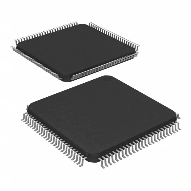
Infineon Technologies CY9BF416NPMC-G-JNE2 — Discrete Semiconductors

CY9BF416NPMC-G-JNE2 Infineon FM3 MCU, ARM Cortex-M3 144MHz

MPNCY9BF416NPMC-G-JNE2
End of Life

Infineon FM3 MB9B410R series ARM® Cortex®-M3 32-bit MCU, CY9BF416NPMC-G-JNE2, 144 MHz, 512 KB Flash, 64 KB RAM, CANbus, EBI/EMI, 83 I/O, 100-LQFP, -40 to 85°C, ROHS3.

$8.41Ref. price · indicative, final on quote
Packaging100-LQFP
StockContact for availability
MOQ1 pcs
  • 100% new & originalTraceable channels only — no refurbs, no pulls, no remarked parts.
  • Date & lot codes on quoteStated per line before you commit; label photos on request.
  • MSL-compliant ESD packingMoisture-sealed bags with indicator cards; reels photo-verified.
  • PayPal buyer protectionPay by T/T, PayPal or Payoneer — card payments covered end to end.

Specifications

CY9BF416NPMC-G-JNE2 Technical Specifications
ParameterValue
SeriesFM3 MB9B410R
Mounting typeSurface Mount
Oscillator typeInternal
Program memory typeFLASH
Voltage - supply (Vcc (Vdd))2.7V ~ 5.5V
Operating temperature-40°C ~ 85°C (TA)
Speed144MHz
PackageTray
RAM size64K x 8
Core size32-Bit Single-Core
PeripheralsDMA, LVD, POR, PWM, WDT
ConnectivityCANbus, CSIO, EBI/EMI, I²C, LINbus, UART/USART
Number of i (O)83
Core processorARM® Cortex®-M3
Case100-LQFP
Data convertersA/D 16x12b
Program memory size512KB (512K x 8)

Product details

144 MHz Cortex-M3 with CAN and external bus — what the BOM gets

The Infineon CY9BF416NPMC-G-JNE2 is a 32-bit ARM Cortex-M3 MCU clocked at 144 MHz. It carries 512 KB of Flash program memory and 64 KB of SRAM, with a full set of peripherals including DMA, PWM, watchdog, and a 16-channel 12-bit ADC.

144 MHz speed — real-time control headroom

The 144 MHz core clock on a Cortex-M3 gives this part the interrupt latency and throughput to handle a motor-drive current loop or a CAN gateway forwarding frames without stalling. Compared to the 80 MHz XMC4200 in the same class, this is nearly double the processing budget for control algorithms or protocol stacks.

512 KB Flash + 64 KB SRAM — firmware sizing for production

512 KB of Flash and 64 KB of SRAM define the firmware ceiling. For a typical industrial controller running a real-time OS, a CANopen stack, and a Modbus RTU slave, this provides comfortable headroom for field-upgradeable application code without resorting to external memory. The 64 KB SRAM is enough for multi-packet DMA buffers and a modest heap.

CANbus and EBI/EMI — dual-domain bridging

The CY9BF416NPMC-G-JNE2 integrates a CANbus controller alongside an external bus interface (EBI/EMI). This combination lets the MCU bridge a CAN fieldbus to a parallel-memory peripheral — an FPGA, a display controller, or a second MCU — without an external bridge chip. It saves board area and BOM cost in gateway or HMI designs where a separate CAN-to-parallel converter would otherwise be needed.

Lifecycle and compliance

Infineon lists the CY9BF416NPMC-G-JNE2 as Active with no end-of-life notice. ROHS3 compliant. For a production BOM being frozen today, this part carries no LTB risk and no PCN watch for near-term obsolescence.

Frequently asked questions

What is an equivalent replacement for the CY9BF416NPMC-G-JNE2?

The closest functional sibling is the CY9BF314RPMC-G-JNE2 from the FM3 MB9B310R series. It shares the same ARM Cortex-M3 core at 144 MHz, the same 100-LQFP footprint, and the same peripheral set except it drops EBI/EMI and adds USB. The CY9BF314R is a pin-compatible drop-in for designs that do not need the external bus but want USB connectivity.

What is the CY9BF416NPMC-G-JNE2's speed rating?

The core runs at 144 MHz. That is the maximum clock for the ARM Cortex-M3 on this device, and it determines the interrupt latency and throughput for real-time control loops or protocol processing.

Is the CY9BF416NPMC-G-JNE2 RoHS compliant?

Yes. Infineon certifies it as ROHS3 Compliant. The suffix -JNE2 indicates the lead-free / RoHS-compliant plating option.