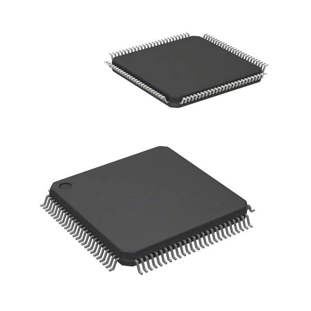
Infineon Technologies CY9BF404NAPMC-G-UNE2 — Logic ICs

CY9BF404NAPMC-G-UNE2 ARM Cortex-M3 MCU, 80 MHz, 256 KB Flash

MPNCY9BF404NAPMC-G-UNE2
End of Life

Infineon FM3 MB9B400A series CY9BF404NAPMC-G-UNE2, 32-bit ARM Cortex-M3 MCU, 80 MHz, 256 KB Flash, 32 KB RAM, CANbus, 80 I/O, 100-LQFP, -40°C to 85°C.

$10.48Ref. price · indicative, final on quote
Packaging100-LQFP
StockContact for availability
MOQ1 pcs
  • 100% new & originalTraceable channels only — no refurbs, no pulls, no remarked parts.
  • Date & lot codes on quoteStated per line before you commit; label photos on request.
  • MSL-compliant ESD packingMoisture-sealed bags with indicator cards; reels photo-verified.
  • PayPal buyer protectionPay by T/T, PayPal or Payoneer — card payments covered end to end.

Specifications

CY9BF404NAPMC-G-UNE2 Technical Specifications
ParameterValue
SeriesFM3 MB9B400A
Mounting typeSurface Mount
Oscillator typeInternal
Program memory typeFLASH
Voltage - supply (Vcc (Vdd))2.7V ~ 5.5V
Operating temperature-40°C ~ 85°C (TA)
Speed80MHz
PackageTray
RAM size32K x 8
Core size32-Bit Single-Core
PeripheralsDMA, LVD, POR, PWM, WDT
ConnectivityCANbus, CSIO, EBI/EMI, I²C, LINbus, UART/USART
Number of i (O)80
Core processorARM® Cortex®-M3
Case100-LQFP
Data convertersA/D 16x12b
Program memory size256KB (256K x 8)

Product details

The 80 I/O count in a 100-LQFP package gives enough headroom for a sensor array or a local HMI without moving to a larger footprint.

The Flash is enough for a CANopen stack, a Modbus RTU handler, and a few hundred lines of application logic. The 32 KB SRAM leaves room for a couple of large buffers — a 1 KB CAN mailbox plus a 2 KB UART FIFO, for example — without running into allocation pressure. If the firmware needs a full TCP/IP stack or a GUI frame buffer, the 32 KB SRAM becomes the tight constraint; that is the design decision to check before committing the BOM line.

For a new design going into a five- to ten-year production run, this removes the sourcing risk that comes with NRND or obsolete parts. The ROHS3 compliance is current for EU and global markets.

CANbus and industrial connectivity — what the peripheral set covers

The CANbus interface is the standout connectivity feature here. It is a full CAN 2.0 controller, so pairing it with an external transceiver (like a TJA1050 or SN65HVD230) gives a node that talks on a 125 kbps to 1 Mbps bus. The peripheral list also includes DMA, LVD, POR, PWM, and WDT — the usual set for a motor-drive or power-conversion controller. The 16-channel 12-bit ADC can sample current-sense resistors or thermistors without an external ADC.

Frequently asked questions

Is CY9BF404NAPMC-G-UNE2 compatible with CAN bus?

Yes. The MCU includes a CANbus controller as part of its connectivity set. It requires an external CAN transceiver (e.g., TJA1050) to connect to a physical CAN bus. The controller supports standard CAN 2.0 frames.

What is the operating frequency of CY9BF404NAPMC-G-UNE2?

The core operates at 80 MHz. That is the maximum clock speed for the ARM Cortex-M3 core on this device.