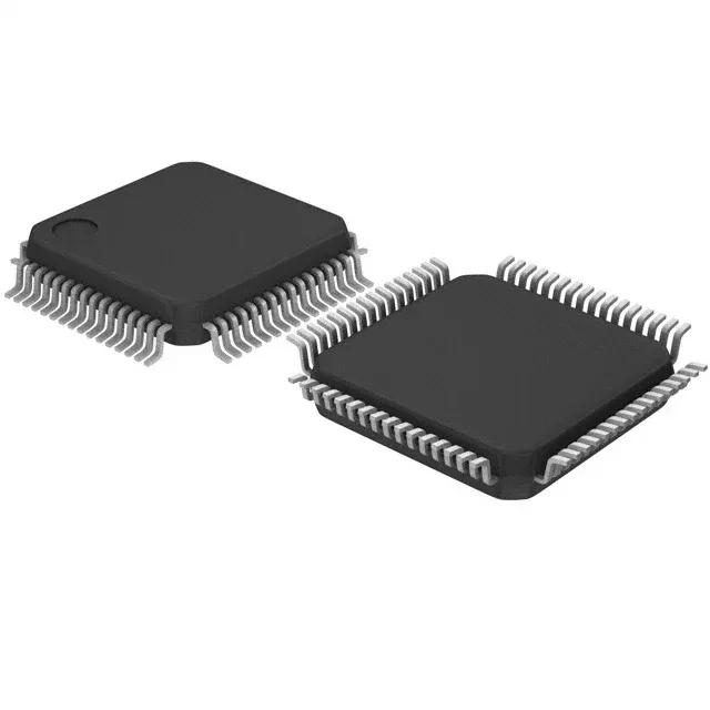
Cortex-M4F at 160 MHz — real-time headroom for motor-drive and sensor-fusion loops
The CY9BF364LPMC1-G-JNE2 is an Infineon FM4 MB9B360L series microcontroller built around an ARM Cortex-M4F core running at 160 MHz. The floating-point unit (FPU) on the M4F handles sensor-fusion math or motor-control transforms without a software emulation penalty — the 32-bit single-cycle MAC and hardware divide keep the loop jitter low enough for field-oriented control at 20 kHz PWM rates. That single-supply flexibility simplifies the board power tree — one rail feeds the core, the I/O ring, and the internal oscillators. With 288 KB of flash and 32 KB of SRAM, the firmware budget is sized for a communication stack (USB + LIN + UART) plus a moderate application layer. The 32 KB RAM is tight for a full TCP/IP stack with large buffers, but it is comfortable for a CANopen or Modbus RTU node running a control loop.
Peripheral set for a fieldbus node or sensor hub
Connectivity includes USB, LIN, I²C, UART/USART, and CSIO — enough to bridge a sensor array to a fieldbus gateway or to act as a motor-drive controller with a CAN interface. The 15-channel 12-bit ADC and dual 10-bit DAC let it read analog sensors and output analog setpoints without an external converter. On-chip peripherals include DMA, LVD, POR, PWM, and WDT — the DMA offloads the CPU for periodic ADC reads or UART transfers, while the LVD and POR handle brown-out recovery without external supervisor ICs. The PWM module is suitable for driving a 3-phase inverter bridge with dead-time insertion handled in hardware. For precision timing (USB full-speed or a CAN bit clock), an external resonator or crystal can still be connected to the dedicated pins.
Temperature grade and board-fit note
The 64-LQFP package (10×10 mm, 0.5 mm pitch) requires a 4-layer PCB for reliable fan-out of the inner rows — a 2-layer board will struggle with the signal integrity on the 48 I/O pins. The 48 I/O count is enough for a sensor hub with a parallel LCD interface or a motor-drive control board with encoder inputs, but it is not a high-pin-count part — if your design needs 80+ GPIO, the FM3 sibling CY9BF314RPMC-G-JNE2 (103 I/O) is the alternative, though it uses a Cortex-M3 core at 144 MHz and a different package.
Active production — no lifecycle risk for new designs
The FM4 MB9B360L series is a mainstream Infineon MCU line with broad distribution support. It is not a pin-compatible drop-in — the package and core differ — but it shares the same peripheral set (DMA, LVD, POR, PWM, WDT) and supply voltage range. If you need more I/O or a lower temperature grade, that is the migration path.