Core architecture and clock
The CY9AF141NBPQC-G-JNE2 is an ARM Cortex-M3 MCU from Infineon's FM3 MB9A140NB series, clocked at 40 MHz. The Cortex-M3 pipeline delivers 1.25 DMIPS/MHz, so the effective throughput is about 50 DMIPS — enough for real-time control loops in motor drives or PLC I/O modules without an external co-processor.
On-chip memory budget
64 KB of Flash (64K x 8) and 16K x 8 of SRAM. The Flash holds the application binary and bootloader; the SRAM covers the stack, heap, and data buffers. For a typical Modbus RTU slave or a simple PID loop, 64 KB Flash leaves room for a RTOS kernel plus the application layer. The 16K x 8 SRAM is tight for heavy frame buffering — budget it against your largest DMA transfer.
Package and board integration
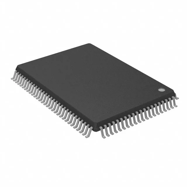
Housed in a 100-BQFP (PQFP) with a 14x20 mm body. The 0.65 mm pitch is hand-solderable in rework but benefits from a stencil for production. 83 I/O are brought out — enough for a 7-segment display bank, keypad matrix, and a parallel LCD interface without a port expander.
Peripheral set and connectivity
On-chip peripherals include LVD, POR, PWM, and WDT — the watchdog and brown-out reset are essential for unattended industrial controllers. Connectivity covers CSIO, EBI/EMI, I²C, SPI, and UART/USART. The 24-channel 12-bit ADC (A/D 24x12b) samples analog inputs like thermocouples or potentiometers without an external ADC.
Infineon lists this part as Active. It is ROHS3 compliant.