Mid-range control MCU with industrial temperature margin
40 MHz is a deliberate mid-range choice. It is fast enough to run a field-oriented control loop for a BLDC motor at 10 kHz PWM update or handle a Modbus RTU stack with a 1 ms tick, but it does not carry the power and layout cost of a 120 MHz+ part. The Cortex-M3 core includes a hardware single-cycle multiply and a 12-cycle divide, so the 40 MHz clock still gives you about 0.8 DMIPS/MHz — roughly 32 DMIPS total. That is enough for most real-time control tasks without needing a cache or a prefetch buffer. The Flash wait state is 0 at 40 MHz, so there is no pipeline stall penalty on tight loops.
512 KB of Flash is generous for a mid-range MCU. It holds a full FreeRTOS or ThreadX kernel plus a TCP/IP stack, a CANopen or Modbus application layer, and still leaves room for a bootloader with OTA staging. The 32 KB SRAM is the tighter resource — enough for a few 1 KB communication buffers and a modest heap, but you will need to watch dynamic allocation if you are running a GUI or a large data logger. The RAM is organised as 32K x 8, so it maps cleanly to byte-addressable variables and stack.
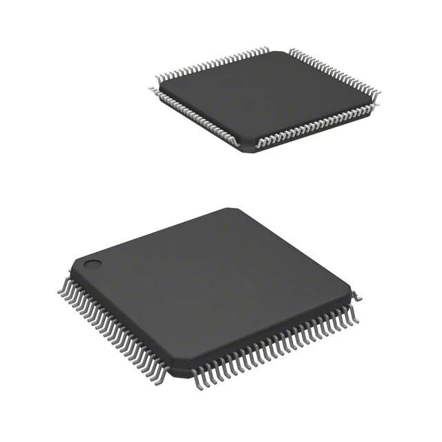
100-LQFP package — footprint and thermal notes
The 83 I/O lines fan out to the perimeter, so a two-layer PCB can route most signals if the layout is planned.
Connectivity and peripherals for industrial control
The 16-channel 12-bit ADC samples at a rate typical for the class — enough for current sensing on a three-phase motor (three shunt resistors, three phase voltages) with channels left over for thermistors and a potentiometer.