What the dual-core clocking means for your BOM
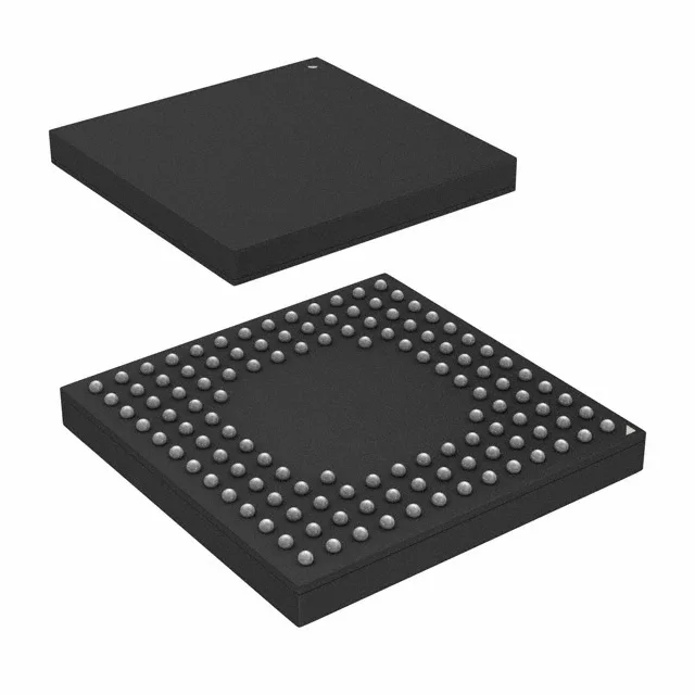
The Infineon CY8C624AAZI-S2D44 is a PSoC 6 32-bit dual-core MCU pairing an ARM Cortex-M0+ at 100 MHz with an ARM Cortex-M4F at 150 MHz. The M0+ handles low-power background tasks — sensor polling, CapSense scanning, communication stack — while the M4F runs the application payload. This asymmetric architecture lets you size the BOM around a single device instead of a two-chip MCU plus companion, saving board area and reducing qualification overhead. Program memory is 2 MB Flash (2M x 8) backed by 1M x 8 SRAM, giving you room for a full RTOS, wireless stacks, and OTA staging without external memory. The 102 I/O count in a 128-TQFP (14x20 mm) package keeps routing manageable on a four-layer board.
No last-time-buy risk on the horizon.
On-chip peripherals include CapSense touch sensing, I²S audio, LCD segment drive, brown-out detect, LVD, POR, PWM, and WDT. Connectivity covers eMMC/SD/SDIO, FIFO, I²C, IrDA, LINbus, Microwire, SmartCard, SPI, SSP, UART/USART, and USB — enough to interface with sensors, displays, wireless modules, and industrial fieldbuses without external bridge chips. Data converters: 16-channel 12-bit SAR ADC, a 10-bit sigma-delta ADC, and two 7/8-bit DACs. The dual ADC types let you sample fast analog signals (SAR) alongside low-frequency, high-resolution measurements (sigma-delta) on the same die.