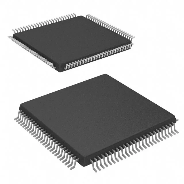
Infineon Technologies CY8C5888AXI-LP096 — Logic ICs

Infineon CY8C5888AXI-LP096 PSoC 5 MCU, 80MHz ARM Cortex-M3

MPNCY8C5888AXI-LP096
End of Life

Infineon PSoC® 5 CY8C58LP series, CY8C5888AXI-LP096, 32-bit ARM Cortex-M3 single-core MCU, 80MHz, 256KB Flash, 64K x 8 SRAM, 2K x 8 EEPROM, 100-LQFP/TQFP, -40°C to 85°C.

$28.95Ref. price · indicative, final on quote
Packaging100-LQFP
StockContact for availability
MOQ1 pcs
  • 100% new & originalTraceable channels only — no refurbs, no pulls, no remarked parts.
  • Date & lot codes on quoteStated per line before you commit; label photos on request.
  • MSL-compliant ESD packingMoisture-sealed bags with indicator cards; reels photo-verified.
  • PayPal buyer protectionPay by T/T, PayPal or Payoneer — card payments covered end to end.

Specifications

CY8C5888AXI-LP096 Technical Specifications
ParameterValue
SeriesPSOC® 5 CY8C58LP
Mounting typeSurface Mount
Oscillator typeInternal
Program memory typeFLASH
Voltage - supply (Vcc (Vdd))1.71V ~ 5.5V
Operating temperature-40°C ~ 85°C (TA)
Speed80MHz
PackageTray
RAM size64K x 8
Core size32-Bit Single-Core
EEPROM size2K x 8
PeripheralsCapSense, DMA, LCD, POR, PWM, WDT
ConnectivityCANbus, I²C, LINbus, SPI, UART/USART, USB
Number of i (O)62
Core processorARM® Cortex®-M3
Case100-LQFP
Data convertersA/D 1x20b, 2x12b; D/A 4x8b
Program memory size256KB (256K x 8)

Product details

What this PSoC 5 brings to a mixed-signal control board

It integrates a programmable analog front end (including a 20-bit delta-sigma ADC, two 12-bit SAR ADCs, and four 8-bit DACs) and digital peripherals such as CapSense touch sensing, CANbus, USB, and multiple serial interfaces. With 62 I/O brought out to a 100-TQFP package, it is a fit for human-machine interface panels, industrial sensor hubs, and motor-control boards where one chip handles touch, display, and fieldbus comms.

The 80 MHz core clock gives this part a throughput edge over the PSoC 4 family (48 MHz Cortex-M0) while keeping power lower than a 150 MHz Cortex-M4 like the CY8C6137BZI-F54. For a design that needs CANbus or USB throughput alongside CapSense scanning, the 80 MHz engine keeps the bus margin comfortable without oversizing the silicon. The 62 I/O count in a 100-TQFP means you get enough pins for a parallel LCD or a memory-mapped display plus the serial interfaces, all in a package that is hand-solderable and inspectable — no BGA rework cost.

Frequently asked questions

What is the maximum speed of CY8C5888AXI-LP096?

The core runs at 80 MHz. At that speed the flash wait state must be set correctly in the boot code to avoid hard faults on tight loops.

What development tools work with CY8C5888AXI-LP096?

Standard ARM Cortex-M3 toolchains (Keil MDK, IAR EWARM, GCC) and Infineon's PSoC Creator IDE support this device. The SWD debug port stays alive even with the watchdog enabled, which simplifies bring-up.

What is the closest functional second-source for CY8C5888AXI-LP096?

Within the Infineon portfolio, the CY8C6137BZI-F54 (PSoC 6, Cortex-M4 at 150 MHz) offers a performance upgrade but is not a pin-compatible drop-in — it moves to a BGA package and adds QSPI. For a same-package alternative, the CY8C4245LQI-483 (PSoC 4, Cortex-M0 at 48 MHz) shares the CapSense and serial interface set but with less memory and no CANbus.