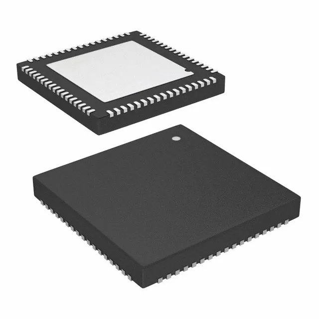
Infineon Technologies CY8C5867LTI-LP025 — Microcontrollers & Processors (MCU / MPU / DSP)

Infineon CY8C5867LTI-LP025 PSoC 5 MCU, 67 MHz, 128 KB Flash

MPNCY8C5867LTI-LP025
End of Life

Infineon Technologies PSoC® 5 CY8C58LP ARM Cortex-M3 MCU, CY8C5867LTI-LP025, 67 MHz, 128 KB FLASH, 32K x 8 RAM, 2K x 8 EEPROM, 38 I/O, 68-VFQFN Exposed Pad, Tray.

$21.52Ref. price · indicative, final on quote
Packaging68-VFQFN Exposed Pad
StockContact for availability
Lead timeIn Stock wk
MOQ1 pcs
  • 100% new & originalTraceable channels only — no refurbs, no pulls, no remarked parts.
  • Date & lot codes on quoteStated per line before you commit; label photos on request.
  • MSL-compliant ESD packingMoisture-sealed bags with indicator cards; reels photo-verified.
  • PayPal buyer protectionPay by T/T, PayPal or Payoneer — card payments covered end to end.

Specifications

CY8C5867LTI-LP025 Technical Specifications
ParameterValue
SeriesPSOC® 5 CY8C58LP
Mounting typeSurface Mount
Oscillator typeInternal
Program memory typeFLASH
Voltage - supply (Vcc (Vdd))1.71V ~ 5.5V
Operating temperature-40°C ~ 85°C (TA)
Speed67MHz
PackageTray
RAM size32K x 8
Core size32-Bit Single-Core
EEPROM size2K x 8
PeripheralsCapSense, DMA, LCD, POR, PWM, WDT
ConnectivityI²C, LINbus, SPI, UART/USART
Number of i (O)38
Core processorARM® Cortex®-M3
Case68-VFQFN Exposed Pad
Data convertersA/D 1x20b, 1x12b; D/A 4x8b
Program memory size128KB (128K x 8)

Product details

The CY8C5867LTI-LP025: This is a design-in viable part, not a shortage-era scavenge. The PSoC 5 toolchain and SDK are mature; the part ships in tray packaging and the 68-QFN footprint is standard across the CY8C58LP family.

67 MHz Cortex-M3 with 128 KB flash — memory budget check

The ARM Cortex-M3 core runs at 67 MHz — enough for a capacitive-touch HMI polling at 100 Hz while the DMA engine moves ADC results into SRAM without CPU intervention. The 128 KB flash holds the application binary plus a bootloader; the 32 KB SRAM leaves roughly 12-16 KB for the stack and heap after the HAL and a small RTOS footprint. The 2 KB EEPROM stores calibration constants and failsafe parameters without wearing the flash sectors.

20-bit ADC and CapSense — analog front-end for sensor fusion

The data converter block includes a 20-bit delta-sigma ADC and a separate 12-bit SAR ADC — the 20-bit channel handles precision strain-gauge or thermocouple inputs, while the 12-bit SAR scans multiple analog channels at higher throughput. Four 8-bit DACs provide analog set-points or waveform generation. The CapSense peripheral implements self- and mutual-capacitance touch sensing without an external touch controller; the DMA engine streams the raw counts to SRAM for post-processing. The 38 general-purpose I/O include the CapSense shield electrode and the LCD segment drive — the LCD controller drives up to 4 commons and 32 segments directly.

PSoC 5 vs PSoC 6 — what the Cortex-M4 peer changes

The CY8C6137BZI-F54 runs a Cortex-M4 at 150 MHz with 104 I/O and a 1.7 V supply — it is not a pin-drop replacement. The 68-QFN footprint of the CY8C5867LTI-LP025 does not map to the PSoC 6's 124-ball BGA; a board spin is required. For a BOM that already qualifies the CY8C5867LTI-LP025, the Cortex-M3 part remains the correct fit unless the application needs the M4's DSP extension or the higher I/O count.

Frequently asked questions

What is the closest functional second-source to the CY8C5867LTI-LP025?

The CY8C6137BZI-F54 is a PSoC 6 Cortex-M4 part running at 150 MHz with 104 I/O, but it uses a 124-ball BGA package — the 68-QFN footprint of the CY8C5867LTI-LP025 is not compatible. The 20-bit ADC and 4x8-bit DAC on the CY8C5867LTI-LP025 are not present on the PSoC 6 peer. A board spin is required to migrate.

What compliance documentation does Infineon provide for the CY8C5867LTI-LP025?

Infineon confirms ROHS3 compliance for this part. Standard documentation includes the datasheet, application notes, and the PSoC Creator IDE with component datasheets.