ARM Cortex-M3 at 67 MHz with programmable analog
The CY8C5668AXI-LP010 is a PSoC 5 device from the CY8C56LP series, built around an ARM Cortex-M3 core running at 67 MHz.
Peripheral set and I/O count for mixed-signal designs
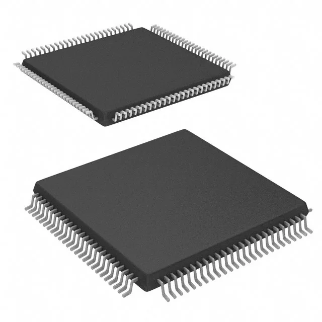
With 62 I/O lines in a 100-TQFP package (14x14 mm), the CY8C5668AXI-LP010 gives you enough pins for a parallel LCD interface, a bank of CapSense touch inputs, and several serial buses without multiplexing. Connectivity covers I²C, LINbus, SPI, UART/USART, and USB — the USB peripheral handles both device and host roles, which simplifies adding a debug or data-logging port without an external USB bridge chip. The data converter block includes two 12-bit ADCs and four 8-bit DACs, giving you enough analog channels for sensor acquisition and analog output generation on a single chip.
Active production, ROHS3 compliant
No stock-holding claim — each order is sourced per the BOM quantity.
How the CY8C5668AXI-LP010 compares to the PSoC 6 CY8C6137BZI-F54
The CY8C6137BZI-F54 is a PSoC 6 part with a Cortex-M4 core at 150 MHz, more than double the clock speed of this CY8C56LP device. It also offers 104 I/O and 8x12-bit SAR ADCs with a 12-bit DAC, versus the 62 I/O and 2x12-bit ADCs / 4x8-bit DACs here. However, the CY8C5668AXI-LP010 runs on a wider supply range (1.71 V to 5.5 V vs 1.7 V) and includes EEPROM on-chip — the PSoC 6 part omits dedicated EEPROM. If your design needs 5 V-tolerant I/O and non-volatile parameter storage without external EEPROM, the CY8C56LP is the better fit; if you need higher throughput and more analog channels, the CY8C6137BZI-F54 is the step up. The packages are different — 100-TQFP here versus a BGA on the PSoC 6 — so a board respin is required to swap between them. They are not pin-to-pin compatible.