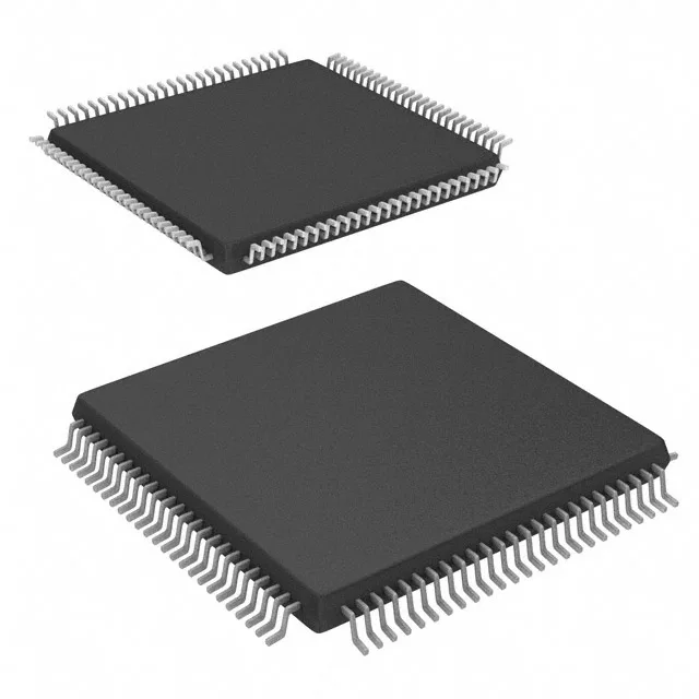
67 MHz Cortex-M3 with programmable analog — the PSOC 5 selection anchor
The CY8C5468AXI-LP106 is an Infineon PSOC 5 device built around a 32-bit ARM Cortex-M3 core clocked at 67 MHz. That clock rate is the throughput ceiling for the application, but the real value is the programmable analog and digital fabric that offloads the CPU — CapSense touch sensing, DMA data movement, LCD drive, PWM generation, and a watchdog timer are all on-chip peripherals that run without core intervention. With 256 KB of program flash and 64 KB of SRAM, this part has room for a moderate application stack — think a sensor hub with a graphical LCD, a motor control loop with fieldbus communication, or a human-machine interface with capacitive touch buttons. The 2 KB EEPROM is separate from the flash, so calibration constants or configuration parameters survive a firmware update without a dedicated EEPROM chip on the board.
Industrial temperature grade and wide supply — design margin for harsh environments
The supply range from 1.71V to 5.5V means this MCU can run directly from a 3.6V Li-ion cell, a 5V regulated rail, or a 1.8V low-power supply without an external regulator — a real BOM simplification when the system has multiple voltage domains. The 0.50 mm pitch on the TQFP is manageable on a 4-layer board; a 2-layer board can break out the outer rows but will struggle with the inner power/ground pads.
ROHS3 compliance is confirmed. For volume production, check with your sourcing contact about reel availability — the tray is standard for engineering samples and low-to-mid volume builds.