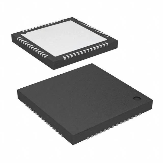
Infineon Technologies CY8C4248LQI-BL583 — Logic ICs

Infineon CY8C4248LQI-BL583 PSoC 4 BLE MCU, 48MHz Cortex-M0

MPNCY8C4248LQI-BL583
End of Life

Infineon PSoC® 4 CY8C4xx8 BLE series, CY8C4248LQI-BL583, ARM Cortex-M0 32-bit MCU, 48MHz, 256KB Flash, 32K x 8 RAM, Bluetooth, CapSense, 36 I/O, 1.71V-5.5V, -40°C to 85°C, 56-UFQFN Exposed Pad.

$8.32Ref. price · indicative, final on quote
Packaging56-UFQFN Exposed Pad
StockContact for availability
MOQ1 pcs
  • 100% new & originalTraceable channels only — no refurbs, no pulls, no remarked parts.
  • Date & lot codes on quoteStated per line before you commit; label photos on request.
  • MSL-compliant ESD packingMoisture-sealed bags with indicator cards; reels photo-verified.
  • PayPal buyer protectionPay by T/T, PayPal or Payoneer — card payments covered end to end.

Specifications

CY8C4248LQI-BL583 Technical Specifications
ParameterValue
SeriesPSOC® 4 CY8C4xx8 BLE
Mounting typeSurface Mount
Oscillator typeInternal
Program memory typeFLASH
Voltage - supply (Vcc (Vdd))1.71V ~ 5.5V
Operating temperature-40°C ~ 85°C (TA)
Speed48MHz
PackageTray
RAM size32K x 8
Core size32-Bit Single-Core
PeripheralsBluetooth, Brown-out Detect/Reset, Cap Sense, DMA LCD, LVD, POR, PWM, SmartCard, SmartSense, WDT
ConnectivityI²C, IrDA, LINbus, Microwire, SmartCard, SPI, SSP, UART/USART
Number of i (O)36
Core processorARM® Cortex®-M0
Case56-UFQFN Exposed Pad
Data convertersA/D 16x12b SAR; D/A 2xIDAC
Program memory size256KB (256K x 8)

Product details

PSoC 4 BLE MCU with integrated Bluetooth and CapSense

The Infineon CY8C4248LQI-BL583 is a PSoC 4 BLE microcontroller from the CY8C4xx8 BLE series, built around an ARM Cortex-M0 core clocked at 48 MHz. The part integrates Bluetooth LE, capacitive touch sensing (CapSense), LCD drive, and a 16-channel 12-bit SAR ADC plus two IDACs, making it a single-chip solution for wireless sensor nodes and human-machine interfaces.

48 MHz Cortex-M0 — throughput and timing

The 48 MHz core clock is the performance ceiling for this device. At this speed, the Cortex-M0 executes most single-cycle instructions, and the Flash controller requires zero wait states for aligned 32-bit reads up to 48 MHz — no wait-state configuration needed unless you push beyond. For BLE stack + application code, the 256 KB Flash leaves room for the Bluetooth stack plus a modest application; the 32 KB SRAM handles BLE packet buffers and a few kilobytes of sensor data. If your application needs more than 32 KB of RAM for large frame buffers or complex analytics, step up to the PSoC 6 family.

Integrated Bluetooth and CapSense — peripheral fit

The 36 GPIOs in the 56-QFN package provide enough pins for a small keypad, a few LEDs, and sensor inputs while leaving serial lines free. The 16-channel 12-bit SAR ADC samples at up to 1 Msps (typical), adequate for most sensor readouts. The two IDACs can generate analog reference currents or drive external loads without an external DAC.

Infineon lists the CY8C4248LQI-BL583 as Active (current production). This part is suitable for qualification into new designs without an imminent obsolescence risk. For dual-sourcing, the CY8C4247LQI-BL473 is a pin-compatible sibling with 128 KB Flash and 8x12b ADC — a drop-in for lower memory or ADC channel count needs.

Frequently asked questions

What is the difference between CY8C4248LQI-BL583 and CY8C4247LQI-BL473?

The CY8C4247LQI-BL473 is a pin-compatible sibling with half the Flash (128 KB vs 256 KB) and an 8-channel 12-bit SAR ADC instead of 16 channels. Both share the same 48 MHz Cortex-M0 core, 32 KB SRAM, BLE, CapSense, and 56-QFN package. The CY8C4248LQI-BL583 is the higher-density option for larger firmware or more analog inputs.

How do I program the CY8C4248LQI-BL583?

Programming uses Infineon's PSoC Creator or ModusToolbox IDE via the SWD (Serial Wire Debug) interface. The part boots from internal Flash with BOOT0 strapped low. The SWD port remains active even with the watchdog enabled, allowing debug access during development.