Active production — no design-in gate
The CY8C4146LQI-S423T: ROHS3 compliant per the manufacturer's declaration, so no exemption paperwork needed for EU or global BOMs.
Cortex-M0+ at 48 MHz — what the core delivers
ARM Cortex-M0+ single-core running at 48 MHz — the standard entry-level 32-bit throughput for sensor-fusion, touch-interface, and low-power control loops. The 64 KB Flash and 8 KB RAM (8K x 8) budget leaves room for a CapSense library, communication stacks, and a modest RTOS footprint. Program memory is Flash — field-upgradable firmware without an external EEPROM for bootloader storage.
CapSense and analog — what the peripheral set actually means
Integrated CapSense controller with 16-channel 12-bit SAR ADC and two IDAC outputs — this is the block that turns a touch-sensor board into a single-chip design. The 10-bit slope ADC is there for low-resolution monitoring; the 12-bit SAR handles the signal-chain work. WDT guards against firmware hangs in unattended equipment.
Supply and temperature — single-rail, industrial range
No second supply needed for the analog peripherals; the internal LDO handles the core. A factory-floor sensor node or outdoor enclosure with passive solar heating stays inside the envelope without active cooling.
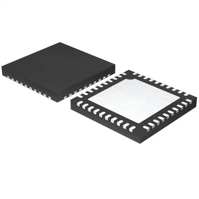
40-QFN 6x6 mm — layout note
Package is 40-UFQFN exposed pad, supplier device package 40-QFN (6x6 mm). The exposed paddle is the ground return for the core and analog — the datasheet's recommended footprint ties it to the ground plane with multiple vias for thermal relief. Without that, the junction temperature rises faster than the 85°C ambient limit suggests. 34 I/O in a 40-pin QFN means most pins are GPIO — useful for a keypad matrix or parallel LCD data bus without needing a port expander.
Serial connectivity — the bus mix
For a sensor hub, the I²C bus talks to the IMU and ambient-light sensor; the UART talks to a host controller or BLE module. LINbus is there for automotive sub-bus nodes, though the temperature grade is industrial, not automotive. Internal oscillator means no external crystal is required for the core clock — two less BOM lines and two less layout constraints. The internal RC is trimmed to ±1% over temperature per the PSoC 4 family specification.