48 MHz Cortex-M0+ with integrated analog — the CapSense and sensor hub MCU
The CY8C4146FNI-S433T is a PSoC 4 part built around a 32-bit ARM Cortex-M0+ core running at 48 MHz. What sets it apart from a generic M0+ MCU is the programmable analog and digital fabric on the same die — the on-chip CapSense block, 12-bit SAR ADC, and dual IDACs mean a capacitive touch interface or analog sensor front-end fits without external converters. 64 KB of flash and 8 KB of RAM are modest by application-processor standards, but they are sized for the single-chip control-and-UI role this part targets: a touch panel with a few sensor inputs, a simple LCD segment display, and a serial link back to a host controller.
WLCSP package — board space drives the package choice
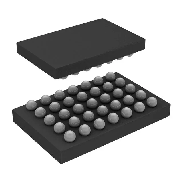
The 35-ball WLCSP (2.11 x 2.6 mm) is the smallest package option in the PSoC 4 CY8C4100S series. At this pitch, the PCB layout must account for the 0.4 mm ball pitch typical of this package class — fan-out via micro-vias or a fine-line layer is expected. The 31 available I/O in this package count is enough for a CapSense matrix plus a serial bus and a few general-purpose signals, but the trade-off is that not every peripheral pin is brought out compared to a QFN variant.