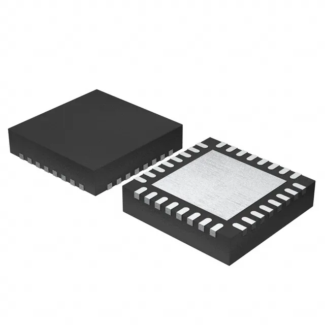
Active lifecycle with a compliance caveat
The CY8C4125LQI-S432: RoHS non-compliant per the manufacturer listing; this matters for EU RoHS enforcement and for contracts that mandate the exemption-free directive. The part ships with the factory's standard five-year warranty through authorized distribution.
Cortex-M0+ core with integrated analog and touch
32-bit ARM Cortex-M0+ core clocked at 24 MHz — the 2-stage pipeline and single-cycle multiply deliver 0.95 DMIPS/MHz, adequate for sensor fusion, HMI polling, and real-time control loops in industrial and consumer embedded systems. 32 KB on-chip flash and 4 KB SRAM — the flash stores a modest firmware stack including a RTOS kernel and CapSense library; the SRAM leaves room for a 1 KB touch-scan buffer plus a few hundred bytes of stack and variable space. Analog front-end includes a 16-channel 10-bit slope ADC and a separate 16-channel 12-bit SAR ADC, plus two IDAC outputs. The slope ADC is well suited for low-frequency capacitive sensing scans; the SAR ADC handles higher-speed sensor readings at up to 1 Msps. CapSense peripheral is the headline block — the CY8C4100S series is built around Cypress's fifth-generation capacitive touch sensing, supporting self-capacitance and mutual-capacitance electrodes. LCD segment drive is also integrated for direct glass displays without an external controller.
Supply flexibility and serial connectivity
The wide range also covers battery-discharge down to 1.71 V. Serial interfaces include I²C (master/slave), SPI, UART/USART, LINbus 2.1, IrDA, Microwire, and SmartCard — the SCB (Serial Communication Block) can be reconfigured in firmware to any of these protocols, reducing BOM by eliminating external protocol converters. 27 general-purpose I/O lines in the 32-QFN package — the exposed pad provides a low-inductance ground return for the analog peripherals and aids thermal dissipation when the MCU drives external loads.
Industrial temperature grade and package footprint
32-UFQFN exposed pad package, 5x5 mm body — the 0.5 mm pitch QFN footprint is standard for compact sensor nodes, wearable HMI panels, and space-constrained IoT edge devices.