Core architecture and memory envelope
The CY8C4045LQI-S411 is a 32-bit single-core MCU built around the ARM Cortex-M0+ processor running at 48 MHz — the M0+ pipeline delivers 0.95 DMIPS/MHz, so the throughput ceiling is roughly 45 DMIPS before flash wait-states factor in. On-chip program memory is 32 KB of Flash (32K x 8), paired with 4K x 8 of SRAM. The 4 KB RAM footprint suits lightweight sensor-node or CapSense front-end applications where the stack and a few buffers fit; anything requiring a large frame buffer or RTOS heap will push against this ceiling.
Supply flexibility and peripheral set
Connectivity covers I²C, IrDA, LINbus, Microwire, SmartCard, SPI, SSP, and UART/USART — enough serial interfaces for a mixed-protocol sensor hub or human-machine interface panel.
Package, footprint, and temperature grade
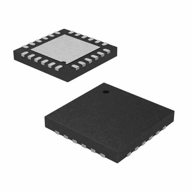
Housed in a 24-UFQFN with exposed pad, the supplier device package is 24-QFN (4x4 mm). The 19 general-purpose I/O count is the total available on this 24-pin package — each I/O can be mapped to the CapSense, serial, or timer functions via the programmable routing matrix, but the 19-pin ceiling means a design needing more than 19 external signals must move to a larger package variant in the CY8C4000S family.
No official second-source cross-reference exists from Infineon, but the part is a single-sourced PSOC 4 device.