What the 24 MHz Cortex-M0+ and 32 KB flash mean for your BOM
The CY8C4025FNI-S412T runs a single-core ARM Cortex-M0+ at 24 MHz — enough throughput for a capacitive touch interface polling a dozen CapSense channels while managing an I²C sensor bus and a UART debug link without timing pressure. The 32 KB flash and 4 KB RAM (4K x 8) hold a modest firmware image with a CapSense tuning table and a few hundred bytes of runtime data; if your application logs sensor readings or runs a GUI frame buffer, budget the RAM against the stack and heap before committing.
Peripheral fit: CapSense, serial interfaces, and LCD drive
This part integrates CapSense — Cypress/Infineon's capacitive touch-sensing block — so a membrane button or proximity slider connects directly to the MCU pins without a separate touch controller. The LCD peripheral drives segment-based glass displays, eliminating a separate LCD driver IC in a low-cost HMI panel.
Package reality: 25-WLCSP at 2.02x1.93 mm
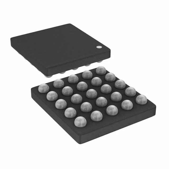
The 25-WLCSP (wafer-level chip-scale package) measures 2.02 x 1.93 mm — roughly the area of a grain of rice. The 21 I/O fan out on a fine-pitch ball grid; a 4-layer PCB with microvias is the practical minimum for routing all signals without via-in-pad. No exposed thermal pad — heat dissipates through the solder balls and the board copper; keep the ground plane continuous under the package.
Temperature grade and supply flexibility
A sensor node in an outdoor enclosure or a factory-floor HMI sees this range; an engine-bay or hot-side application above 85°C needs a different grade.