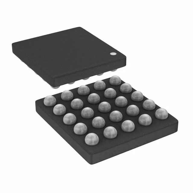
Infineon Technologies CY8C4025FNI-S402T — Microcontrollers & Processors (MCU / MPU / DSP)

Infineon CY8C4025FNI-S402T PSOC 4 MCU, 24MHz, 32KB Flash

MPNCY8C4025FNI-S402T
End of Life

Infineon Technologies PSOC® 4 CY8C4000S series ARM® Cortex®-M0+ 32-Bit MCU, CY8C4025FNI-S402T, 24MHz, 32KB FLASH, 4K x 8 RAM, 21 I/O, 25-WLCSP package, -40°C to 85°C.

$2.71Ref. price · indicative, final on quote
Packaging25-XFBGA, WLCSP
StockContact for availability
Lead timeIn Stock wk
MOQ1 pcs
  • 100% new & originalTraceable channels only — no refurbs, no pulls, no remarked parts.
  • Date & lot codes on quoteStated per line before you commit; label photos on request.
  • MSL-compliant ESD packingMoisture-sealed bags with indicator cards; reels photo-verified.
  • PayPal buyer protectionPay by T/T, PayPal or Payoneer — card payments covered end to end.

Specifications

CY8C4025FNI-S402T Technical Specifications
ParameterValue
SeriesPSOC® 4 CY8C4000S
Mounting typeSurface Mount
Oscillator typeInternal
Program memory typeFLASH
Voltage - supply (Vcc (Vdd))1.71V ~ 5.5V
Operating temperature-40°C ~ 85°C (TA)
Speed24MHz
PackageTape & Reel (TR); Cut Tape (CT)
RAM size4K x 8
Core size32-Bit Single-Core
PeripheralsBrown-out Detect/Reset, CapSense, LCD, LVD, POR, PWM, WDT
ConnectivityI²C, IrDA, LINbus, Microwire, SmartCard, SPI, SSP, UART/USART
Number of i (O)21
Core processorARM® Cortex®-M0+
Case25-XFBGA, WLCSP
Data convertersA/D 1x10b
Program memory size32KB (32K x 8)

Product details

24 MHz Cortex-M0+ with on-chip CapSense

The CY8C4025FNI-S402T: This core delivers enough throughput for sensor polling, UI control, and communication protocol handling in a single chip. On-chip peripherals include CapSense touch sensing, LCD drive, PWM, and a brown-out detect/reset — the CapSense block alone can replace a separate touch controller in human-interface applications like capacitive buttons or sliders. The 32 KB flash and 4 KB RAM (4K x 8) set the firmware budget: the flash holds the application code and constant data, while the RAM handles stack, heap, and small buffers. For designs needing more than a few kilobytes of runtime data, plan for external memory or a higher-tier PSOC 4 variant.

WLCSP package and board integration

The 25-WLCSP package (2.02 x 1.93 mm) is a wafer-level chip-scale package with solder balls directly on the die — no molded body. This shrinks the footprint to the bare die size, which helps in space-constrained designs like wearables or sensor modules, but the 0.4 mm ball pitch demands careful PCB layout with via-in-pad or microvia fan-out. The wide range means a single regulator can feed the MCU without a secondary LDO, simplifying the power tree.

Connectivity and I/O budget

The I²C and SPI interfaces allow daisy-chaining sensors or EEPROMs, while the UART handles debug or fieldbus bridging. The single 10-bit ADC limits analog input channels — if the application needs more than one analog sensor, an external analog mux or a PSOC 4 part with more ADC channels (like the CY8C4245LQI-483 with 8x12-bit) is the migration path.

ROHS3 compliant, meeting the latest EU restriction-of-hazardous-substances directive. No additional compliance documentation (REACH, UL, IEC) is listed in the available records.

Frequently asked questions

Is CY8C4025FNI-S402T a drop-in replacement for CY8C4245LQI-483?

No — the CY8C4245LQI-483 uses a 48-pin QFN package (7x7 mm) with 34 I/O, while the CY8C4025FNI-S402T is a 25-ball WLCSP (2.02x1.93 mm) with 21 I/O. The pinout, footprint, and ball map are different; a board spin is required. The CY8C4245 also runs at 48 MHz and has 8x12-bit ADC versus the 1x10-bit ADC here.