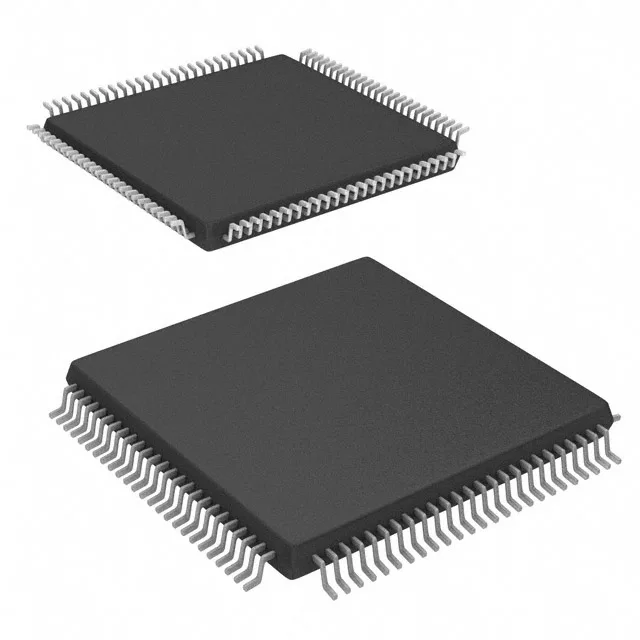
8051 core at 67 MHz with programmable analog
The CY8C3666AXI-037 is an 8-bit MCU built around the 8051 core clocked at 67 MHz, part of the PSoC 3 family. The 67 MHz clock on an 8051 pipeline gives roughly 60 MIPS throughput — the limiting factor for loop-heavy control code is the flash wait-state profile, not the core itself. For mixed-signal tasks, the on-chip data converters include a 16-channel 12-bit ADC and a 4-channel 8-bit DAC, so many sensor-conditioning and analog-output loops close without an external converter.
Peripheral set for human-interface and industrial comms
On the connectivity side: CANbus, EBI/EMI, I²C, LINbus, SPI, and UART/USART — enough to talk to a fieldbus gateway, a local display, and a sensor array on the same chip. With 62 general-purpose I/O in the 100-TQFP package, the pinout can serve a parallel LCD data bus, a row-column keypad matrix, and several serial interfaces simultaneously without external GPIO expanders.
The fine pitch demands a 4-layer PCB for reliable fan-out of the 62 I/O — two-layer boards will struggle to route the inner rows without vias under the package. Surface-mount assembly with a standard reflow profile; the package is ROHS3 compliant per the lifecycle record.