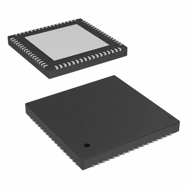
Infineon Technologies CY8C3246LTI-149 — Microcontrollers & Processors (MCU / MPU / DSP)

Infineon CY8C3246LTI-149 PSOC 3 MCU, 50MHz, 64KB Flash

MPNCY8C3246LTI-149
End of Life

Infineon Technologies PSOC® 3 CY8C32xx series 8-bit MCU, CY8C3246LTI-149, 50MHz, 64KB Flash, 8K x 8 RAM, 2K x 8 EEPROM, 68-VFQFN Exposed Pad, Tray.

$12.0Ref. price · indicative, final on quote
Packaging68-VFQFN Exposed Pad
StockContact for availability
Lead time3-5 Days wk
MOQ1 pcs
  • 100% new & originalTraceable channels only — no refurbs, no pulls, no remarked parts.
  • Date & lot codes on quoteStated per line before you commit; label photos on request.
  • MSL-compliant ESD packingMoisture-sealed bags with indicator cards; reels photo-verified.
  • PayPal buyer protectionPay by T/T, PayPal or Payoneer — card payments covered end to end.

Specifications

CY8C3246LTI-149 Technical Specifications
ParameterValue
SeriesPSOC® 3 CY8C32xx
Mounting typeSurface Mount
Oscillator typeInternal
Program memory typeFLASH
Voltage - supply (Vcc (Vdd))1.71V ~ 5.5V
Operating temperature-40°C ~ 85°C (TA)
Speed50MHz
PackageTray
RAM size8K x 8
Core size8-Bit
EEPROM size2K x 8
PeripheralsCapSense, DMA, LCD, POR, PWM, WDT
ConnectivityEBI/EMI, I²C, LINbus, SPI, UART/USART
Number of i (O)38
Core processor8051
Case68-VFQFN Exposed Pad
Data convertersA/D 16x12b; D/A 1x8b
Program memory size64KB (64K x 8)

Product details

50 MHz 8051 core with on-chip programmable analog

The CY8C3246LTI-149 is an 8-bit MCU built around the 8051 core running at 50 MHz, part of the PSOC® 3 CY8C32xx family from Infineon Technologies.

Memory, connectivity, and peripheral headroom

Program memory is 64 KB of Flash (64K x 8), backed by 2 KB of EEPROM for non-volatile parameter storage and 8 KB of SRAM for data buffers and stack. The 64 KB Flash ceiling suits firmware images that include a bootloader plus a moderate application layer — a typical CapSense-based UI or sensor-fusion algorithm fits without external memory. The 38 I/O lines are multiplexed with the CapSense, LCD segment drive, and PWM outputs, so the actual usable I/O count depends on which peripherals are enabled — a full LCD segment drive can consume 16–24 pins, leaving 14–22 for general-purpose use. The data converter block provides 16 multiplexed inputs to a single 12-bit SAR ADC, plus a separate 8-bit DAC. The ADC sample rate is not listed in the summary, but the 12-bit resolution and 16-channel mux are typical for reading multiple analog sensors (potentiometers, thermistors, strain gauges) on a single conversion cycle.

Frequently asked questions

What is the closest functional second-source to the CY8C3246LTI-149?

The CY8C4245LQI-483 is a PSOC 4 device with an ARM Cortex-M0 core running at 48 MHz, 32-bit architecture, and a different peripheral set (8x12b ADC, 2x IDAC). It is not pin-compatible — the CY8C4245LQI-483 comes in a 68-QFN package but the pinout and supply voltage range differ. A board respin is required for migration; there is no drop-in replacement for the CY8C3246LTI-149 from the PSOC 4 family.

What compliance documentation does Infineon provide for the CY8C3246LTI-149?

The device is ROHS3 compliant per the lifecycle record. Infineon provides a standard datasheet, application notes, and a PCN notification channel for this PSOC 3 series.