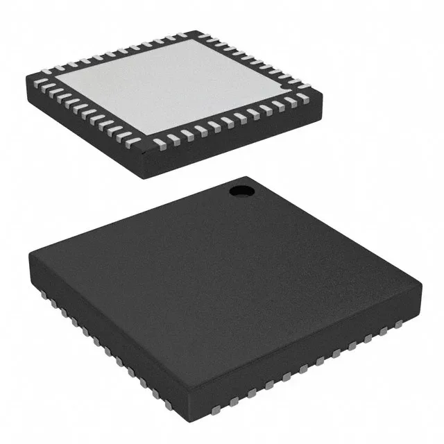
24 MHz M8C core with 16 KB flash — the memory ceiling for a single-loop controller
The CY8C28645-24LTXI runs an 8-bit M8C core at 24 MHz. That clock drives the CPU, not the peripheral bus — the ADC conversion rate and PWM resolution are derived from the system clock, so a 24 MHz ceiling means the 14-bit ADC samples at roughly 48 ksps max (one conversion per 500 cycles). For a sensor read-and-react loop reading one analog channel and updating a PWM output, the loop budget is about 20 µs before the next sample arrives. Program memory is 16 KB flash, RAM is 1K × 8. That is a tight fit for a USB stack or a full Modbus RTU implementation — the flash holds roughly 4,000 instructions at 4 bytes per instruction. The 1 KB SRAM leaves about 800 bytes after the stack and interrupt vectors, which is enough for a 16-entry FIFO of 50-byte records but not for a frame buffer larger than a VGA character cell.
Analog front-end: 4×14-bit ADC, 4×9-bit DAC — resolution mismatch matters
The data-converter block packs four 14-bit ADCs and four 9-bit DACs. The 14-bit ADC gives 16,384 counts over the supply range — at 3.3 V reference, one LSB is 201 µV. That is enough for a strain-gauge bridge with a gain stage, but the ADC input impedance is about 10 kΩ during sampling; the source must settle within 1 µs for a 14-bit accurate reading. The 9-bit DAC outputs 512 levels — fine for a setpoint voltage or a VCO tune line, not for audio or precision bias. The ADC offset drifts about ±5 LSB over that span per the PSoC1 family datasheet typical curve — budget this into the calibration routine if the sensor is at the cold end and the reference is at room temperature.
Supply and package: 3-5.25 V with exposed-pad QFN
Supply voltage is 3 V to 5.25 V. The part runs on a single rail — no separate analog supply. Without that, the junction-to-ambient thermal resistance rises above 40°C/W, and at 5.25 V drawing about 15 mA the die self-heats 6°C above ambient — acceptable at 85°C ambient but marginal at 105°C (which the part is not rated for). The package is a 48-QFN 7×7 mm. The pitch is 0.5 mm; the exposed pad is on the bottom. Reflow profile per JEDEC J-STD-020: peak temperature 260°C, time above 217°C is 60-150 seconds. The part is ROHS3 compliant, so no exemption for lead in solder — standard SAC305 paste works.
Peripherals and GPIO: 44 pins with LVD, POR, PWM, WDT
On-chip peripherals include LVD, POR, PWM, and WDT. The POR threshold is 2.95 V typical — at 3.0 V supply the part is already in the brown-out region; the LVD can be set to 2.85 V to trigger an interrupt before the POR fires. The WDT runs from the internal oscillator and times out at 16 ms minimum; the firmware must pet it every 8 ms or the part resets. There are 44 GPIOs. The QFN package routes them to the perimeter pads — no dedicated analog pins; any GPIO can be configured as an analog input via the PSoC switched-capacitor block. The IrDA connectivity uses a UART with a pulse-shaping circuit; the external IR transceiver still needs a 3 mm LED and a photodiode.
Lifecycle and sourcing: active, no NRND flag
The closest peer in the same PSoC1 family is the CY8C29566-24AXIT, which runs the same M8C core at 24 MHz but packs 32 KB flash and 2 KB SRAM in a 48-pin TQFP. The CY8C28645 has 16 KB flash and 1 KB SRAM — the CY8C29566 doubles both. The package difference (QFN vs TQFP) means the PCB footprint is not compatible; a board spin is required to swap between them. The CY8C29466-24PVXI is also a 24 MHz M8C part but in a 28-pin SSOP with only 24 GPIO — a drop-in replacement only if the design uses fewer than 24 I/O and fits the smaller package.