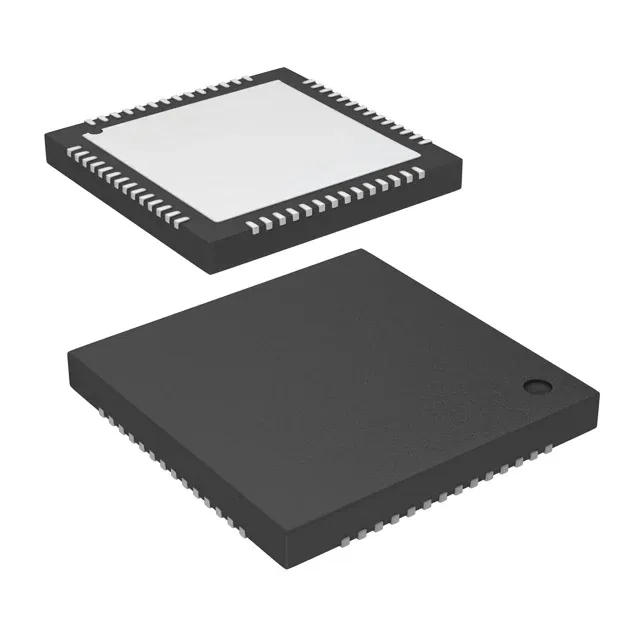
Infineon Technologies CY8C24894-24LTXIT — Microcontrollers & Processors (MCU / MPU / DSP)

Infineon CY8C24894-24LTXIT PSOC 8-Bit MCU, 24MHz, 16KB Flash

MPNCY8C24894-24LTXIT
End of Life

Infineon Technologies PSOC®1 CY8C24xxx 8-bit MCU, CY8C24894-24LTXIT, M8C core 24MHz, 16KB FLASH, 1K x 8 RAM, 50 I/O, 47x14b ADC, USB, 56-QFN-EP 8x8mm, -40 to 85°C.

$9.54Ref. price · indicative, final on quote
Packaging56-VFQFN Exposed Pad
StockContact for availability
Lead timeIn Stock wk
MOQ1 pcs
  • 100% new & originalTraceable channels only — no refurbs, no pulls, no remarked parts.
  • Date & lot codes on quoteStated per line before you commit; label photos on request.
  • MSL-compliant ESD packingMoisture-sealed bags with indicator cards; reels photo-verified.
  • PayPal buyer protectionPay by T/T, PayPal or Payoneer — card payments covered end to end.

Specifications

CY8C24894-24LTXIT Technical Specifications
ParameterValue
SeriesPSOC®1 CY8C24xxx
Mounting typeSurface Mount
Oscillator typeInternal
Program memory typeFLASH
Voltage - supply (Vcc (Vdd))3V ~ 5.25V
Operating temperature-40°C ~ 85°C (TA)
Speed24MHz
PackageTape & Reel (TR); Cut Tape (CT)
RAM size1K x 8
Core size8-Bit
PeripheralsPOR, PWM, WDT
ConnectivityI²C, SPI, UART/USART, USB
Number of i (O)50
Core processorM8C
Case56-VFQFN Exposed Pad
Data convertersA/D 47x14b; D/A 2x9b
Program memory size16KB (16K x 8)

Product details

47-channel ADC array — the analog edge

The CY8C24894-24LTXIT: The 47-channel, 14-bit successive-approximation ADC is the headline peripheral on this die. It samples across the full 3.0 to 5.25 V supply range without an external reference — the internal bandgap is trimmed at test. For a multi-sensor data logger or a capacitive touch panel scanning 47 nodes, the ADC front-end eliminates the external mux and the second op-amp stage.

Memory envelope and the M8C pipeline

16 KB flash (16K x 8) with 1 KB SRAM. The M8C core fetches instructions at 24 MHz with zero wait states from the flash at 3.3 V and above; below 3.0 V the flash controller inserts one wait state, dropping the effective throughput. The 1 KB RAM is the hard limit for stack, data buffers, and the USB endpoint descriptor table — a firmware image that allocates a 512-byte USB FIFO leaves 512 bytes for everything else.

USB and serial connectivity on one die

The USB 2.0 full-speed (12 Mbps) peripheral shares the die with I2C, SPI, and UART/USART blocks. The USB PHY runs from the internal oscillator — no external crystal required for USB operation, though the internal oscillator accuracy (±2.5 % over temp) limits the USB frame timing margin. For a design that bridges a legacy UART sensor to a USB host, this part eliminates the separate USB-to-UART bridge IC.

Industrial temperature and supply range

Rated -40 to 85 °C ambient with a 3.0 to 5.25 V supply. The POR and WDT peripherals are active across the full voltage range; the brown-out threshold is set at 2.85 V typ.

The part is ROHS3 compliant. Sourced through authorized and independent distribution; lead time and pricing confirmed at RFQ. No official pin-compatible successor exists — the PSOC 1 family has no direct drop-in replacement from Infineon, so the BOM position is tied to this order code for the life of the design.

Frequently asked questions

What is the closest pin-compatible alternative to CY8C24894-24LTXIT?

There is no official pin-compatible successor from Infineon for this PSOC 1 device. The 56-QFN-EP footprint is specific to this die; a different PSOC 1 variant in the same package may have a different peripheral mix or memory size, but the pinout is not guaranteed identical across the family. A board spin would be required to migrate to a different MCU family.

What compliance documentation does Infineon provide for CY8C24894-24LTXIT?

Infineon certifies ROHS3 compliance. Standard documentation includes the datasheet, application notes, and the PSOC 1 register reference manual. No UL, IEC, or AEC-Q qualification is listed for this part.