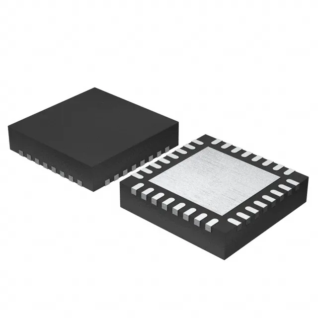
PSoC 1: configurable analog and digital on an 8-bit M8C core
The Infineon CY8C24423A-24LTXI is an 8-bit PSoC 1 microcontroller from the CY8C24xxx family, built around the proprietary M8C core running at 24 MHz. What sets this part apart from a plain 8051 or PIC is the integrated configurable analog and digital blocks: it carries a 10-channel 14-bit ADC and two 9-bit DACs on-chip, plus programmable digital blocks that can implement timers, PWMs, UARTs, SPI, or I²C without external glue logic. This makes it a single-chip solution for sensor conditioning, human-interface, and mixed-signal control applications where a separate op-amp and ADC would otherwise consume board area and BOM cost.
4 KB Flash and 256 bytes RAM — budget accordingly
Program memory is 4 KB Flash, and data RAM is 256 x 8 bytes. That is a tight firmware envelope: the PSoC Designer configuration code for the analog and digital blocks shares the same Flash, so a complex CapSense or ADC scan routine leaves little room for a RTOS or large lookup tables. This part is sized for a single-purpose control loop — think a temperature transmitter, a capacitive touch button panel, or a small motor controller — not a feature-rich application with a GUI stack.
Industrial temperature range and wide supply
The supply voltage spans 2.4V to 5.25V, so it can run directly from a 3.6V Li-ion cell, a regulated 3.3V rail, or a 5V industrial bus without an extra LDO.
For a BOM line that was qualified years ago, this is the best news: no end-of-life scramble, no requalification cycle.
Pin-compatible family and second-source reality
Within the CY8C24xxx family, the CY8C24423A sits at the mid-density tier. The CY8C29466-24PVXI is a pin-compatible upgrade path within the same PSoC 1 architecture — it doubles the program memory and adds more analog channels (12x14b ADC, 4x9b DAC) while keeping the same 24 MHz M8C core and peripheral set. If your firmware fits in 4 KB and you need the smaller 32-QFN footprint, the CY8C24423A is the correct fit; the CY8C29466 is worth evaluating for a next-revision BOM if code size or analog channel count becomes a constraint.