48-channel 14-bit ADC — the analog edge in an 8-bit MCU
The Infineon CY8C24094-24BVXI is an 8-bit M8C microcontroller from the PSOC®1 CY8C24xxx family, packing a 24 MHz core with 16 KB Flash program memory. Its standout feature is the analog front-end: 48 channels of 14-bit A/D conversion and two 9-bit D/A outputs, a density usually found on much larger parts. That makes this device a natural fit for multi-sensor acquisition — think capacitive touch arrays, environmental monitoring, or industrial sensor fusion where you need to digitise dozens of analog inputs without external muxes.
The M8C core at 24 MHz is a pipelined 8-bit architecture with a single-cycle multiply-accumulate. For a firmware engineer bringing up the part, the internal oscillator means no external crystal is needed for the core clock — one less BOM line. The flash wait state at 24 MHz is zero, so instruction fetches run at full speed. If you are porting code from an earlier PSoC 1 part, the register map and digital blocks are consistent across the CY8C24xxx family, so the bring-up log should look familiar: BOOT0 strapping, SWD debug port, and the watchdog timer defaulting to off.
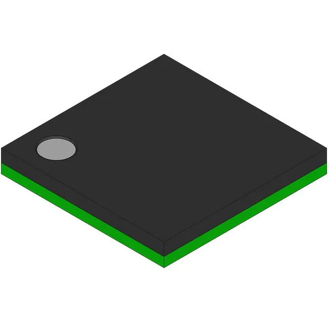
100-VFBGA — layout and rework considerations
The 100-ball VFBGA (Very Fine-pitch Ball Grid Array) gives you 56 usable I/O in a compact footprint, but it demands careful PCB layout. The fine pitch means via-in-pad or microvias are recommended for routing out the inner balls. Reflow profile follows standard lead-free solder (SnAgCu) with a peak temperature around 245°C. The thermal pad at the centre of the package carries the bulk of the dissipation; stitch vias to a ground plane are needed if the part is running at the full 24 MHz with all ADC channels active.
For a BOM cost engineer, that removes the single-source risk flag for the MCU line — you can qualify this part into production without worrying about an imminent EOL. If you need a dual-source hedge, the PSoC 1 family has several pin-compatible density options (e.g., the CY8C29566-24AXIT with 40 I/O and 4x9b DAC), but the 100-VFBGA footprint is unique to this variant, so a second source would require a board spin.