The Cypress CY7C4291V-10JXC is a synchronous FIFO memory with a 1.125 Mbit (128K x 9) organization, designed for high-speed data buffering in systems that need to match data rates between a fast producer and a slower consumer — or vice versa. It clocks at 100 MHz with an 8 ns access time, which means the read and write operations happen on the clock edge, not on asynchronous strobes. The 9-bit width (8 data bits plus a parity or control bit) is common in serial backplane and TDM applications where the ninth bit carries a frame marker or out-of-band flag. The part supports depth and width expansion, so you can cascade multiple devices for deeper or wider buffers without external logic.
The CY7C4291V-10JXC is listed as obsolete.
No FWFT — what that means for read timing
This FIFO does not support First-Word Fall-Through (FWFT). In standard synchronous FIFO operation, the first word written to an empty FIFO is not available on the output pins until the read clock edge that follows the write — there is a one-cycle latency penalty on the first read. FWFT eliminates that latency by presenting the first word immediately after it is written. If your application requires zero-latency read access to the first data word, you would need a FWFT-capable FIFO instead.
32-PLCC package — footprint and layout notes
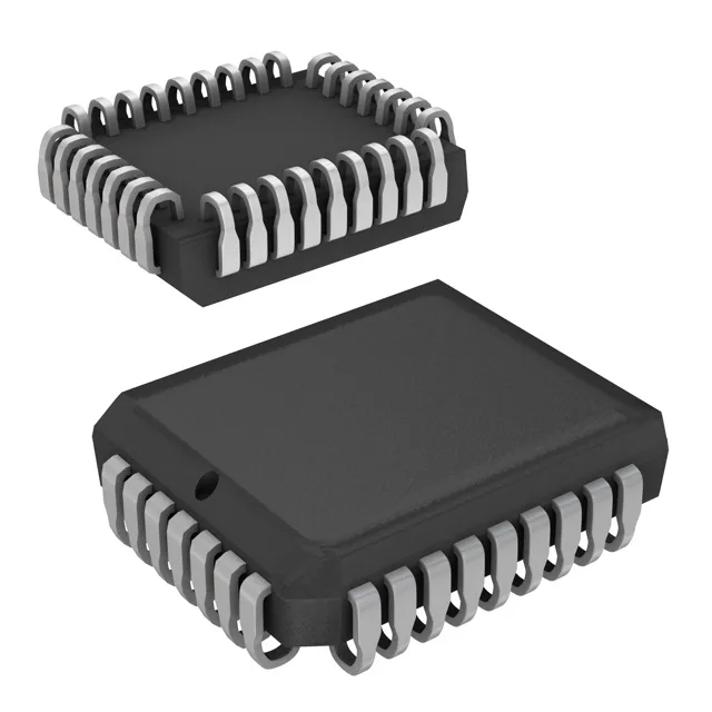
The CY7C4291V-10JXC comes in a 32-lead PLCC (J-Lead) package, supplier device package 32-PLCC (11.43x13.97 mm). This is a surface-mount package with J-shaped leads on all four sides. The PLCC footprint is well-established and socketable — many legacy designs use PLCC sockets for field-serviceability. The J-lead form factor gives good solder-joint reliability under thermal cycling, but the package is not as fine-pitch as TQFP, so routing is straightforward on a two-layer board.