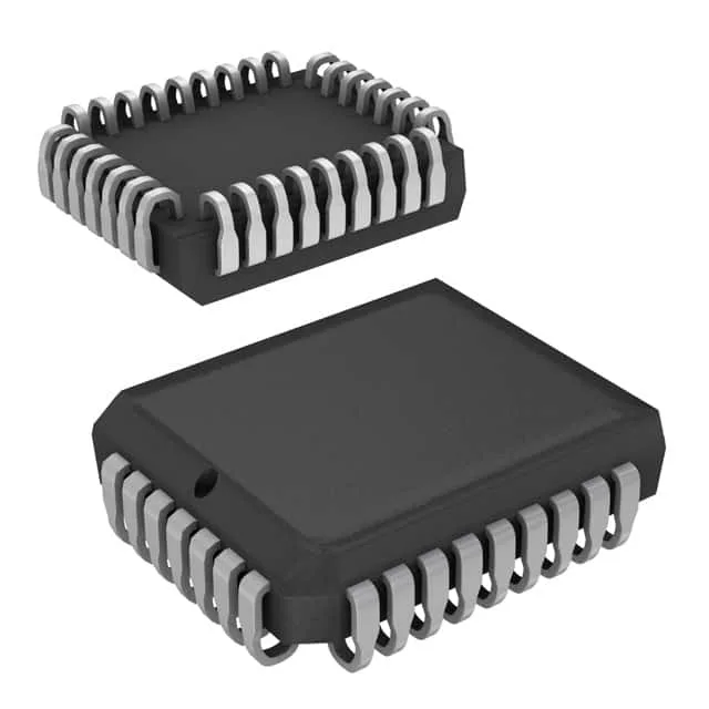
100 MHz synchronous FIFO — 8 ns access, 128K × 9, 5 V legacy rail
The CY7C4291-10JC is a synchronous FIFO from the CY7C series, organized 128K words by 9 bits. The 9th bit is typically used as a parity or control lane alongside the 8-bit data bus — not an extra data byte — so the effective data width is 8 bits plus one flag/parity line. Rated for a 100 MHz data rate with an 8 ns access time, this part clocks data in and out on a single clock edge. The 8 ns access is the time from clock edge to valid data on the output bus — at 100 MHz the 10 ns period leaves 2 ns of margin before the next clock edge, which tightens the board-level timing budget if the trace length or load capacitance adds skew. The 40 mA max supply current is modest for a 5 V FIFO running at 100 MHz, keeping the junction temperature rise within the 70°C ambient envelope.
Obsolete — no direct replacement on record
Infineon lists the CY7C4291-10JC as Obsolete. This means the part is no longer manufactured and has no pin-compatible drop-in from the original manufacturer. For a BOM line that must stay with a 128K × 9 synchronous FIFO in a 32-PLCC footprint, the only path is spot-market procurement.
32-PLCC J-lead — surface-mount, rework-friendly
Housed in a 32-lead PLCC with J-bend leads, body size 11.43 × 13.97 mm. The J-lead footprint is socket-compatible with standard PLCC-32 sockets and is also solderable directly to the PCB. PLCC packages are rework-friendly — a hot-air nozzle or IR station lifts the part cleanly without damaging the board pads, unlike QFP or BGA. The package ships in tube. No retransmit capability and no FWFT (First-Word Fall-Through) support — data flow is standard synchronous: the first word written appears on the output after the first read clock, not immediately. Expansion is supported in both depth and width, allowing multiple devices to cascade.
Programmable flags and synchronous operation
Programmable flags support lets the system set almost-empty and almost-full thresholds in software or via pin strapping — useful for burst control in a data pipeline where the host needs early warning before the FIFO empties or overflows. The flags are synchronous, asserted relative to the clock edge. Bus direction is uni-directional — separate input and output ports, one-way data flow. Expansion type is depth and width, so multiple CY7C4291-10JC devices can be cascaded for larger buffers or wider buses without external logic, using the expansion-in/out pins.