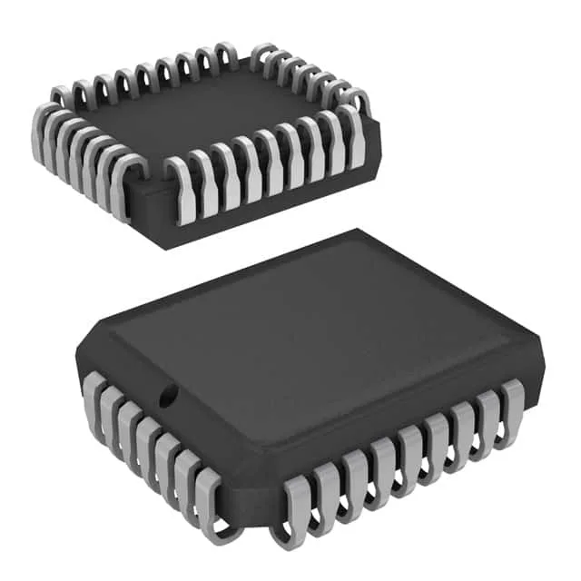
Synchronous FIFO for 100 MHz data-path buffering
The CY7C4261V-10JC is a 144 Kbit (16K x 9) synchronous FIFO from Infineon's CY7C series, designed for unidirectional data buffering at clock rates up to 100 MHz with a corresponding 8 ns access time. The 32-pin PLCC J-Lead package (32-PLCC, 11.43x13.97 mm body) is a through-hole-reflow-compatible surface-mount footprint common in late-1990s to mid-2000s board designs, suitable for rework with a hot-air station and a fine-tip iron.
Timing envelope and buffer depth
The 100 MHz maximum clock rate and 8 ns access time set the cycle budget for the host controller: the FIFO can accept a write or issue a read every 10 ns, with data valid on the output bus 8 ns after the read clock edge. With 16,384 words of 9-bit depth, the FIFO holds 144 Kbit total — enough to buffer one full 16 KB sector plus a parity byte, or to absorb burst mismatches in a 100 MHz data channel where the producer and consumer run at slightly different instantaneous rates. Programmable flags (almost-full, almost-empty) let the system set watermark thresholds via the flag-offset registers, so the host can prefetch or drain before the FIFO hits its full or empty boundary — useful for DMA-driven transfers where latency to service the flag interrupt matters.
The part carries a commercial temperature grade (0°C to 70°C) and comes in a 32-PLCC J-Lead package; no direct pin-compatible replacement is documented in the CY7C family, so a board-level redesign would be needed to migrate to a current-generation FIFO. No last-time-buy window remains open with the factory.