66.7 MHz synchronous FIFO — 144K buffer for unidirectional data paths
The CY7C4261-15JXC is a synchronous FIFO from Infineon's CY7C series, organized as 16K x 9 bits (144K total). It clocks at 66.7 MHz with a 10 ns access time, meaning the read/write cycle repeats every 15 ns — the limiting factor for throughput in a unidirectional data buffer is this cycle time, not the memory depth.
Operating envelope — supply, temperature, and current budget
The commercial temperature grade (0 °C to 70 °C) suits indoor equipment and lab instrumentation; the 35 mA max supply draw means the FIFO's contribution to the board-level thermal budget is negligible even in a densely populated PLCC footprint.
Package and board-fit — 32-PLCC with J-leads
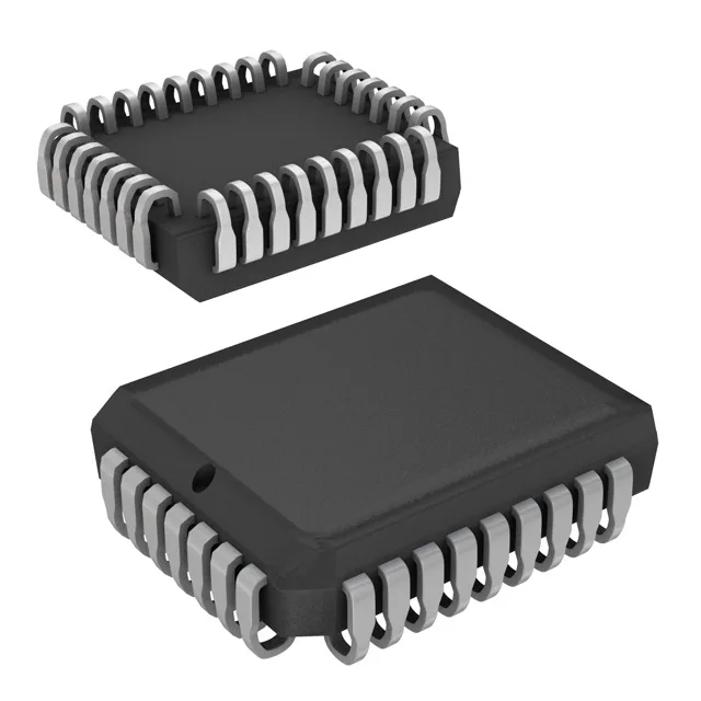
Housed in a 32-lead PLCC (J-lead) package, supplier device package size 11.43 x 13.97 mm. The J-lead form factor allows socketed or soldered mounting on a standard surface-mount pad layout; the 1.27 mm pitch is hand-solderable with a fine tip and does not require a stencil for prototyping. No exposed thermal pad — the die heat dissipates through the leads and the board copper.
Feature set — depth/width expansion, programmable flags, no FWFT
Supports depth and width expansion, so multiple devices cascade for deeper or wider buffers without external logic. Programmable flags let the system set almost-empty and almost-full thresholds to match the host controller's DMA latency. No FWFT (First-Word Fall-Through) and no retransmit capability — the first word is not available on the output pins until the first read clock after the write cycle, and the data cannot be re-read once read out.
Lifecycle reality — obsolete, no successor on record
Infineon lists the CY7C4261-15JXC as obsolete. No official successor part number is published.