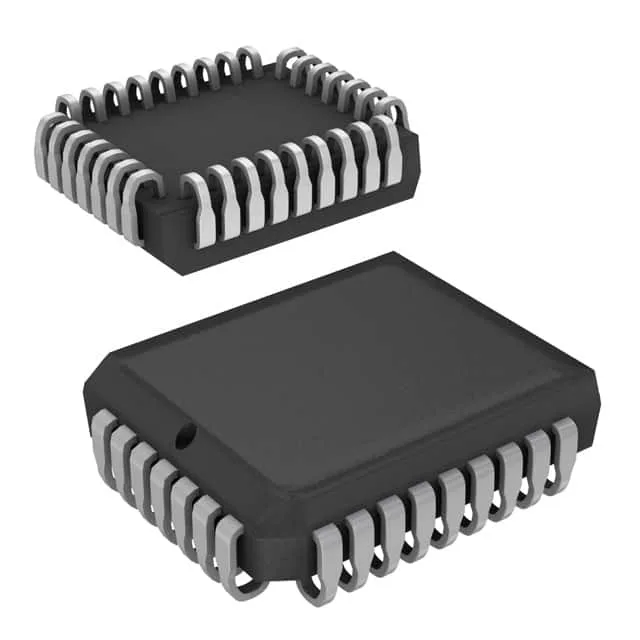
The Cypress CY7C4251-10JXCT is a synchronous FIFO memory in the CY7C series, organized 8K x 9 bits (72K total) and clocked at 100 MHz with an 8 ns access time. This part was designed for moderate-depth buffering in data-acquisition, telecom, and processor-to-peripheral links where a 9-bit width (data plus parity or control) and synchronous clocking keep the bus simple.
8 ns access time — timing margin at 100 MHz
At 100 MHz the clock period is 10 ns. An 8 ns access time leaves 2 ns for setup and hold on the receiving side — tight but workable if the board layout keeps trace lengths matched and the clock jitter under 200 ps. The synchronous interface eliminates the dead cycles you get with asynchronous FIFOs; the read and write pointers advance on the clock edge, so back-to-back transfers are possible. If your system runs slower than 100 MHz, the margin improves proportionally.
72K (8K x 9) — what the depth buys you
8K words of 9 bits each is a moderate buffer depth — enough to absorb bursts in a UART-to-processor link, a parallel ADC data stream, or a small packet buffer. The 9th bit is often used for parity or a control flag. Depth and width expansion are supported, so two or more of these can be cascaded for larger buffers without external logic.
Obsolete — the sourcing reality
This part is listed as obsolete. That means the only channel is surplus or broker stock. If you are repairing a board that uses this FIFO, the scorch mark is probably not on the FIFO itself — check the supply rail first, because the 35 mA max draw rarely kills the chip. For new designs, look at current-generation synchronous FIFOs from Cypress (now Infineon) or compatible parts from IDT/Renesas in the same 32-PLCC footprint, but verify pin compatibility against the datasheet before ordering.
The 32-PLCC (J-Lead) package (supplier device package 32-PLCC 11.43x13.97 mm) is a surface-mount form factor that was common through the 1990s and 2000s. Replacing it on a board requires hot-air rework with a J-lead nozzle; the pads are under the body, so inspection after soldering needs an X-ray or a borescope.