Asynchronous FIFO with 10 ns access — what the speed rating buys you
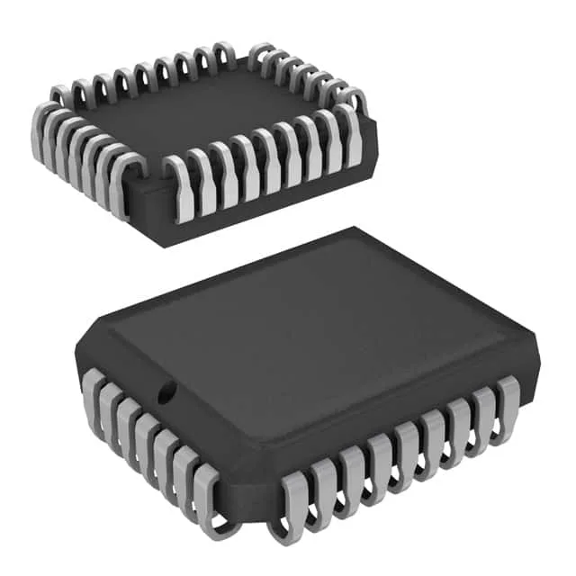
The CY7C425-10JXC is a 9K (1K x 9) asynchronous FIFO from the CY7C series, rated at 50 MHz data rate with a 10 ns access time. The 9-bit width (1K x 9) includes a ninth bit often used for parity or a control flag.
No official successor or second-source is listed. Production has ended; new orders are fulfilled from remaining distributor stock or the spot market. For a BOM line that still specifies this exact order code, procurement must go through independent distribution or a broker. Date codes and package condition (tube, not tape/reel) vary — confirm the visual and electrical quality before ordering.
Retransmit capability and expansion options
Retransmit capability allows the FIFO to re-present data from the first location without a full reset and rewrite — useful for retry protocols or data replay in test equipment. The part supports depth and width expansion for cascading multiple devices, though the asynchronous nature means careful timing on the expansion control signals. No FWFT (First-Word Fall-Through) support means the first word written does not appear on the outputs until a read cycle is issued — the output register holds the previous word until the read flag toggles. No programmable flags — the empty and full flags are fixed thresholds determined by the internal write and read pointers.