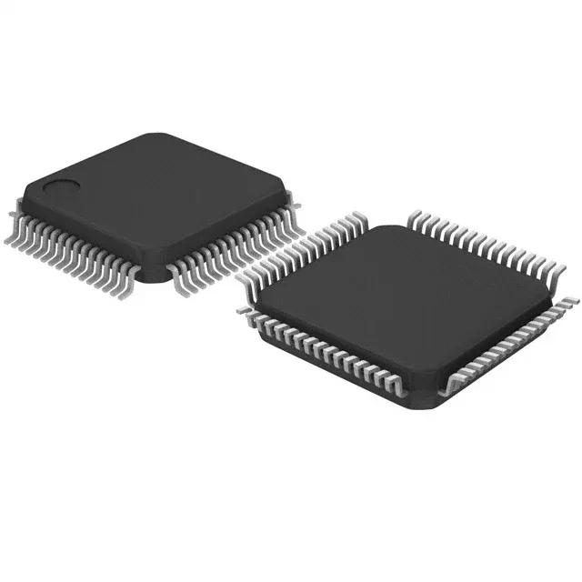
The part supports depth and width expansion, includes programmable flags and retransmit capability, and comes in a 64-LQFP surface-mount package (64-TQFP, 14x14 mm footprint). Typical applications include data buffering in telecom infrastructure, industrial controllers, and high-speed data acquisition systems where a synchronous handshake is needed to match data rates between clock domains.
Obsolete — sourcing through the independent channel
The 10 ns access time at 66.7 MHz leaves a tight but workable window for the downstream logic to latch read data. In a typical synchronous FIFO read cycle, the data appears on the bus within 10 ns of the rising clock edge. That means the receiving device — an FPGA, ASIC, or another FIFO — must have its input setup time satisfied within the remaining clock period minus the access time and any board-level flight delay. For a 66.7 MHz clock (15 ns period), the budget is roughly 5 ns minus trace delay, which is comfortable for most 5 V-tolerant CMOS or LVTTL inputs but leaves no room for slow buffers or long PCB traces.
72K (4K x 18) — sizing the buffer for the job
The 4K x 18 organization means the FIFO holds 4,096 18-bit words. The 18-bit width is a natural fit for 16-bit data plus two control/parity bits, or for 9-bit-wide byte streams with an extra bit for framing. Depth expansion is supported, so multiple devices can be cascaded to build deeper buffers without external logic. Width expansion is also supported, allowing multiple FIFOs to be ganged for wider data paths. The 45 mA maximum supply current is a reasonable budget for a 66.7 MHz synchronous FIFO in a 64-pin LQFP — plan the 5 V rail to deliver at least that per device, plus margin for the expansion logic.