What this FIFO does in a system
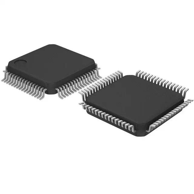
The Cypress CY7C4245-15ASXC is a synchronous FIFO memory with a 4K x 18 organization, clocked at 66.7 MHz and delivering a 10 ns access time. It is designed for unidirectional data buffering between two clock domains or bus widths, common in telecom line cards, DSP coprocessor interfaces, and FPGA-to-backplane bridges. The 18-bit word width accommodates 16-bit data plus two control or parity bits without external muxing. Retransmit capability and programmable flags give the system designer flexible flow control without polling the FIFO status.
66.7 MHz clock and 10 ns access — what they buy you
At 66.7 MHz the FIFO can sustain a 66.7 million words-per-second read or write rate, assuming no flag stalls. The 10 ns access time from the rising clock edge to data valid on the outputs sets the bus timing margin for the receiving logic. With a 15 ns clock period, the 10 ns access leaves 5 ns for PCB trace delay, setup time of the downstream device, and clock jitter — tight but workable with 50-ohm controlled impedance traces under 100 mm. If the receiving FPGA or ASIC has a 2 ns input setup, the margin drops to 3 ns; a board spin or slower speed grade may be needed.
If the design is still in development, consider migrating to a current-production synchronous FIFO in a compatible 64-LQFP footprint, such as the CY7C42xxV series with 3.3 V supply, though pin compatibility must be verified against the specific density and flag options.