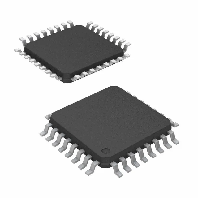
40 MHz synchronous FIFO — bus timing for DSP or packet buffering
The Infineon CY7C4241V-25AXCT is a synchronous FIFO memory from the CY7C series, organized as 4K x 9 bits (36K total). It clocks data in and out at up to 40 MHz, with a 15 ns access time on the read side. No First-Word Fall-Through (FWFT) support means the first read after a write-to-empty transition incurs a latency cycle; for streaming applications, budget that extra clock or use a FWFT-capable part. Programmable almost-full and almost-empty flags let you set watermarks that match your system's burst tolerance, reducing overrun risk without external logic. Depth and width expansion is supported, so multiple devices can be cascaded for larger buffers — no glue needed. The 32-TQFP (7x7 mm) package is a fine-pitch SMD that reflows on standard profiles.
For new designs, look at current-generation synchronous FIFOs from vendors like Renesas or TI — but verify pin-compatibility and timing yourself.
15 ns access time — read-cycle margin on a 40 MHz bus
At 40 MHz, the clock period is 25 ns. The 15 ns access time leaves 10 ns for the read data to propagate from the FIFO output to the receiving register, including PCB trace delay and setup time. That's tight but workable with controlled-impedance routing and short traces (< 50 mm). If your system runs at 50 MHz or higher, this part won't close timing — step up to a faster FIFO (e.g., 10 ns access or better). The 15 ns spec is the max over temperature and voltage, not a typical; budget accordingly.