Synchronous FIFO for clock-domain bridging
It is designed for buffering data between two clock domains in digital systems — think FPGA-to-processor links, DSP data pipelines, or network packet queues where you need a clean read/write handshake without dead cycles.
At 66.7 MHz, the 10 ns access time gives you roughly 5 ns of setup margin after the clock edge — enough for most 5 V logic families (HCT, LVT, or classic ASIC I/O) without adding wait states. If your system runs at the same clock rate but uses slower PLD outputs, budget the access time against the combined propagation delay through the source register and trace flight time.
Obsolete — plan the replacement now
For new designs or volume production, you will need to qualify a replacement — typically a modern synchronous FIFO from the same 5 V supply family, or a dual-clock FIFO IP block inside an FPGA.
Package and supply details for the layout
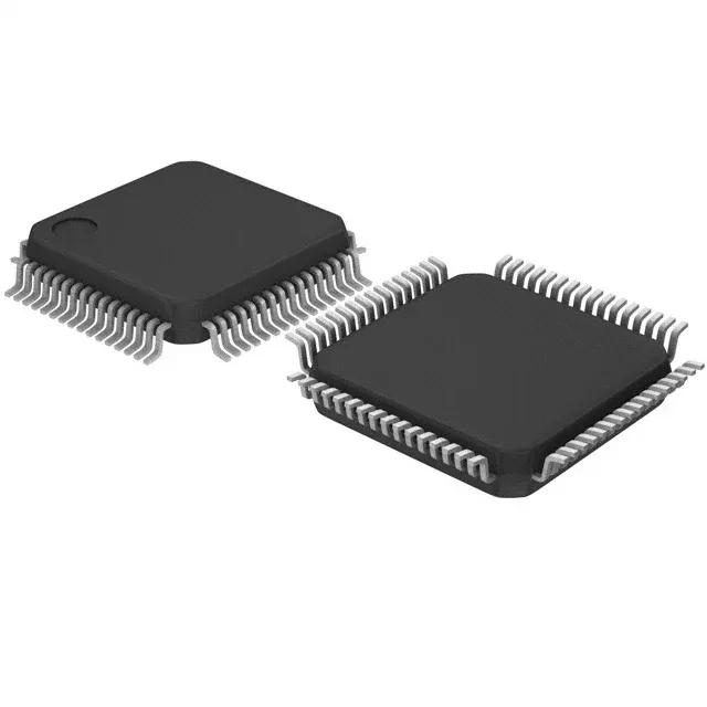
Housed in a 64-LQFP (supplier device package 64-TQFP, 14x14 mm body), this is a surface-mount part with 0.5 mm pitch. Maximum supply current is 45 mA.
Depth and width expansion — no FWFT
The part supports depth and width expansion via cascading multiple devices, but it does not offer First-Word Fall-Through (FWFT) operation. If your design relies on FWFT for zero-latency reads, this is not the right FIFO — look at the Cypress CY7C42X5V series instead. Retransmit capability is present, and programmable flags are supported, giving you flexible almost-full/almost-empty thresholds.