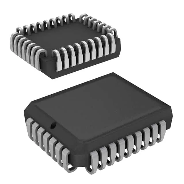
Synchronous FIFO in a 32-PLCC footprint
The Infineon CY7C4221-15JXCT is a 9K (1K x 9) synchronous FIFO memory from the CY7C series, clocked at 66.7 MHz with a 10 ns access time. The part supports depth and width expansion via programmable flags, but lacks FWFT and retransmit capability.
66.7 MHz clock, 10 ns access — what it buys you
The 66.7 MHz synchronous interface means data transfers happen on each clock edge, not on asynchronous read/write strobes — this simplifies the control logic in a system that already has a clock domain at or below that rate. The 10 ns access time is the window from clock edge to data valid on the output bus; at 66.7 MHz (15 ns period) you have 5 ns of setup margin before the next clock edge, enough for moderate board trace lengths without signal-integrity tuning. The 9-bit width (1K x 9) is the classic FIFO depth for 8-bit data plus a parity or control bit — common in telecom framers, serial-to-parallel converters, and glue logic between buses of different widths. The ninth bit can carry an end-of-packet marker or error flag without stealing a data byte. Programmable flags (almost-full, almost-empty) let the system controller pre-empt the FIFO boundary before the hard flags fire — useful for DMA burst termination or interrupt generation at a configurable watermark. Depth and width expansion are supported, so multiple parts can cascade for deeper or wider buffers without external arbitration logic.
Infineon lists the CY7C4221-15JXCT as obsolete.
32-PLCC J-lead — board-fit note
The 32-PLCC package (11.43 x 13.97 mm body) uses J-leads on a 1.27 mm pitch — a standard footprint for PLCC sockets or direct solder. The J-lead profile gives a lower seated height than gull-wing, useful in mezzanine or card-edge assemblies where board-to-board clearance is tight. The package is surface-mount only; no through-hole variant exists for this part.