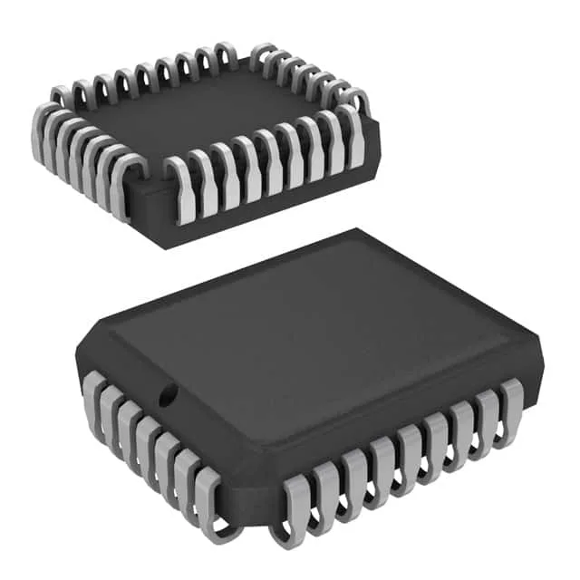
The CY7C421-20JXI: No stock-holding claim is made here.
20 ns access time — timing fit for legacy buses
The CY7C421-20JXI is an asynchronous FIFO with a 20 ns access time and a 50 MHz data rate. This means the read/write cycle completes in 20 ns from the address setup — fast enough to interface with older 5V DSPs, microcontrollers, and ASICs that expect a 50 MHz bus without wait states. Memory depth is 4.5 Kbit organized as 512 words by 9 bits wide. The 9-bit width accommodates an 8-bit data byte plus a parity or control bit — common in telecom framer and legacy datacom designs. The FIFO supports depth and width expansion, so multiple devices can cascade for deeper or wider buffers without external logic. Retransmit capability is also present — a feature that resets the read pointer to the last programmed retransmit boundary, useful in packet retry schemes.
5V supply, industrial temp, 32-PLCC package
This rules out direct drop-in replacement with modern 3.3V or 1.8V FIFOs without a level translator. Packaged in a 32-lead PLCC with J-leads (32-LCC), the supplier device package is 32-PLCC (11.43x13.97 mm). Surface-mount with a standard JEDEC footprint — the J-lead form factor is less common in new designs but well-documented for rework and inspection. Maximum supply current is 90 mA. No FWFT (First-Word Fall-Through) support and no programmable flags — this is a basic asynchronous FIFO with fixed flag logic.