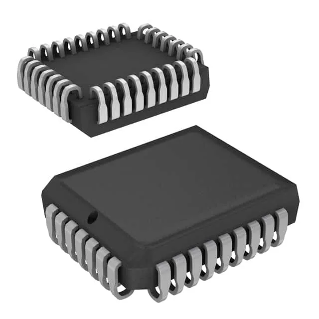
The Cypress CY7C421-20JXCT is a 4.5 Kbit (512 x 9) asynchronous FIFO memory with a 20 ns access time and 50 MHz data rate, designed for rate-matching, buffering, and data aggregation in 5 V logic systems. It supports depth and width expansion for scaling buffer capacity, includes retransmit capability for error recovery, and comes in a 32-PLCC (J-lead) surface-mount package for board-level assembly.
The 20 ns access time and 50 MHz data rate set the read/write cycle window. In a 5 V system with typical 8–10 ns propagation delays from the controller and bus transceivers, the 20 ns access leaves roughly 5–7 ns of setup-and-hold margin at 50 MHz — adequate for synchronous handshaking but tight for backplane expansion. If the design runs multiple FIFOs in cascade, budget the cumulative delay through the depth-expansion logic.
512 x 9 organization — what the extra bit buys you
The 9-bit width (512 x 9) stores an eighth data bit plus a parity or control bit per word, common in 8-bit buses with parity or 9-bit serial protocols. The 4.5 Kbit depth buffers about 512 bytes of burst data — enough for a single Ethernet frame fragment or a few hundred sensor readings, but not for long packet streams. Depth and width expansion are supported, so multiple devices can cascade without external muxing.
Lifecycle reality: obsolete, but sourced to order
The CY7C421-20JXCT is officially obsolete per the manufacturer. For new designs, evaluate the Cypress CY7C42x family (e.g., CY7C421-20JXC in tube or CY7C421-20JXCT in tape-and-reel) as a form-fit-function cross if the stock holds — note that the -20JXC and -20JXCT share the same 32-PLCC (11.43x13.97) footprint and electrical ratings, differing only in packaging medium.