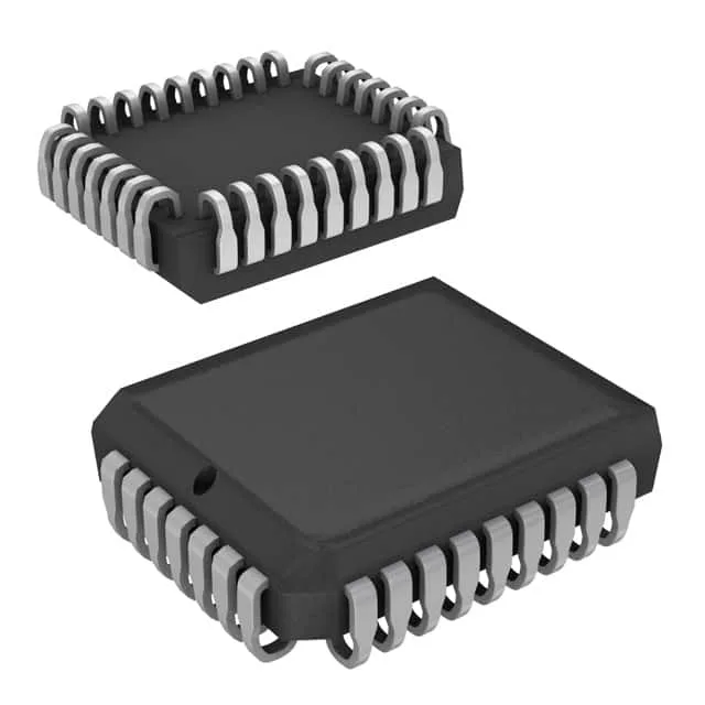
50 MHz asynchronous FIFO in a 32-PLCC package
The Cypress CY7C421-10JXCT is a 4.5 Kbit (512 x 9) asynchronous FIFO memory designed for buffering data between two clock domains or bus widths at up to 50 MHz. Its 10 ns access time gives tight read-cycle timing for legacy 5 V logic systems running at clock rates around 50 MHz. The 9-bit width (8 data bits plus a parity/flag bit) suits it for byte-wide data paths with an extra control line, common in telecom framers, DSP interfaces, and printer controllers from the late-1990s through mid-2000s.
No successor part is listed in the official record. For a BOM line that still calls out this exact order code, procurement should expect to buy against an RFQ from a distributor that stocks legacy FIFOs — availability and pricing vary by date code and remaining inventory. There is no last-time-buy window open; the part is simply no longer manufactured.
In a system clocked at 50 MHz (20 ns period), that leaves 10 ns for the data to propagate through the receiving register's setup-and-hold window — workable with careful PCB trace length matching, but tight if the bus fans out to multiple loads. The 50 MHz data rate is the maximum write/read cycle frequency; the part can sustain back-to-back writes at that rate as long as the FIFO is not full. Depth expansion (cascading multiple devices) is supported via the expansion logic pins, but width expansion requires external glue logic since the bus is unidirectional.
Package and footprint: 32-PLCC (J-Lead)
The part comes in a 32-lead PLCC with J-bend leads (package code 32-LCC), supplier device package 32-PLCC (11.43x13.97 mm). It is a surface-mount package that requires a standard PLCC-32 footprint with a 1.27 mm pitch. The J-lead form gives good coplanarity for reflow, but the package body is a 4-sided JEDEC outline — check your pick-and-place nozzle clearance for the body dimensions.