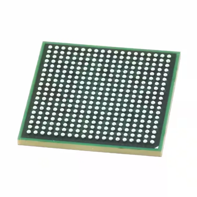
Infineon Technologies CY7C4142KV13-933FCXI — Memory (DRAM / SRAM / Flash / EEPROM)

Infineon CY7C4142KV13-933FCXI QDR IV SRAM, 144 Mbit, 933 MHz

MPNCY7C4142KV13-933FCXI
Active

Infineon CY7C4142KV13-933FCXI, QDR IV synchronous SRAM, 144 Mbit (4M x 36), 933 MHz clock, parallel interface, 1.26V–1.34V supply, industrial -40°C to 85°C, 361-FCBGA (21x21 mm), tray.

$666.6650Ref. price · indicative, final on quote
Sourced new & surplus through independent channelsAuthenticity-screened · ESD-safe packingListing updated Aug 2026

Specifications

CY7C4142KV13-933FCXI specifications
ParameterValue
Memory typeVolatile
MountingSurface Mount
Voltage1.26V ~ 1.34V
Frequency933 MHz
Memory interfaceParallel
Operating temperature-40°C~85°C(TA)
PackageTray
TechnologySRAM - Synchronous, QDR IV
Memory size144Mbit
Memory formatSRAM
Case361-BBGA, FCBGA
Memory organization4M x 36

Product details

933 MHz QDR IV SRAM — 144 Mbit in a 361-FCBGA

The Infineon CY7C4142KV13-933FCXI is a 144 Mbit synchronous SRAM built on the QDR IV architecture, organized as 4M x 36 and clocked at 933 MHz. It is a volatile memory device with a parallel interface, designed for high-bandwidth buffer and cache applications in networking, telecom infrastructure, and high-performance computing.

The 933 MHz clock rate is the defining performance spec for this QDR IV SRAM. At this speed, the memory delivers a data rate of 1.866 Gbps per pin on a double-data-rate bus, which translates to an aggregate bandwidth of roughly 67 GB/s on the 36-bit-wide data path. For a systems architect, this clock frequency drives the signal-integrity budget on the PCB: trace lengths must be matched within a few millimetres, and the 361-FCBGA package demands a controlled-impedance stack-up with adequate decoupling near the BGA balls. The 1.26V to 1.34V core supply is tight — a 1.3V nominal rail with ±3% regulation is typical — so the power design needs a low-noise LDO or a dedicated DC-DC converter with good transient response.

The tray shipping format means the parts arrive in antistatic trays, not tape-and-reel — plan for pick-and-place handling or manual placement if your line is set up for reels.

The base product number CY7C4142 covers a family of QDR IV density and speed variants; if a different density or speed grade is needed, the same footprint and interface apply across the family.

Frequently asked questions

What is the closest pin-compatible alternative to CY7C4142KV13-933FCXI in the QDR IV family?

Within the same QDR IV family, density and speed variants sharing the CY7C4142 base number are pin-compatible across the 361-FCBGA footprint. For a different density (e.g. 72 Mbit or 288 Mbit) or a lower speed grade (e.g. 800 MHz), the same package and interface apply — the datasheet should be consulted for exact timing differences.

Is CY7C4142KV13-933FCXI compatible with QDR II+ interfaces?

No. This is a QDR IV device, which uses a different I/O standard and higher clock rate than QDR II+. The two families are not pin-compatible and require different controller PHYs. Do not substitute a QDR II+ part into a QDR IV socket or vice versa.

What is the lead time for CY7C4142KV13-933FCXI from Infineon?

As an independent distributor, we source across multiple channels and can provide a current lead-time estimate when you submit an RFQ for this part.