QDR-IV SRAM at 1.066 GHz — what the clock rate means for the datapath
The CY7C4142KV13-106FCXC is a 144 Mbit QDR-IV synchronous SRAM from Infineon, organized as 4M x 36 and clocked at 1.066 GHz. That clock frequency is the I/O toggle rate on the address and data buses — the internal memory array runs at a quarter of that speed, but the QDR-IV architecture pipes four 36-bit words per clock cycle, giving a peak read bandwidth of roughly 38.4 Gbit/s per port. The 1.26 V to 1.34 V core supply is tight — a 1.3 V nominal rail with ±3 % regulation keeps the PLL and I/O buffers in spec. The commercial temperature range (0 °C to 70 °C) suits enterprise networking gear, test equipment, and high-end compute accelerators where the ambient is controlled, not automotive or outdoor enclosures.
361-FCBGA package — rework and board integration notes
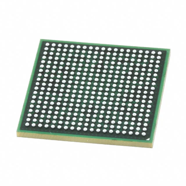
Housed in a 361-ball fine-pitch BGA (FCBGA), 21 mm x 21 mm body. The 1.0 mm ball pitch is manageable with a standard rework station — pre-bake at 125 °C for 8 hours if the tray seal has been broken, per J-STD-033 MSL 3 handling. The surface-mount footprint demands a multi-layer PCB with controlled impedance traces for the 1.066 GHz signalling; the QDR-IV bus is source-synchronous, so trace-length matching on the data and strobe pairs is non-negotiable. Delivered in tray format — not tape-and-reel. For volume pick-and-place, the trays are JEDEC-compatible; for small-batch rework, the FCBGA's solder balls are collapsible with a standard hot-air profile peaking at 245 °C. No lead-free exemption listed; assume RoHS-compliant per Infineon's standard policy.