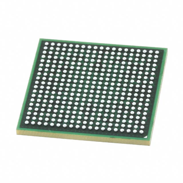
144Mbit QDR IV at 667 MHz — what the clock buys you
The CY7C4141KV13-667FCXC: The 667 MHz clock on this QDR IV SRAM translates to a 1.33 Gbps data rate per pin on the read and write ports, because QDR IV transfers data on both clock edges. That bandwidth targets network switch buffers and high-end compute lookaside tables where the latency of DDR DRAM is a bottleneck. Organized as 4M x 36, the 144Mbit density fits packet buffers in 100 GbE line cards or L3 cache in FPGA-based accelerators — the 36-bit word width matches the internal bus width of many network processors without packing overhead.
Supply rails and temperature — the design constraints
The core supply is a tight 1.26 V to 1.34 V window — a 1.3 V ±3% rail. That means the VRM tolerance plus ripple must stay inside 40 mV peak-to-peak, which typically forces a separate LDO or a multi-phase switcher with remote sense, not a shared 1.2 V or 1.5 V plane. The 0°C to 70°C (TA) commercial temperature grade limits this part to controlled indoor environments — server rooms, central offices, lab equipment. No deployment in outdoor base stations or under-hood automotive without active cooling that keeps the ambient below 70°C.
361-FCBGA — reflow and board integration
The flip-chip construction puts the die face-down on the substrate, so the thermal interface is through the balls, not a top-side heatsink. Plan for tray-fed pick-and-place or manual placement for prototypes.
Active lifecycle — no LTB pressure
That means standard sourcing through authorized distribution is the baseline; no need to broker-surf for inventory. The base product number CY7C4141 covers the QDR IV family; speed and temperature variants share the same footprint. If the 667 MHz speed grade or commercial temp range is tight for your BOM, a -5 or -6 speed grade or industrial temp sibling may swap in without a board spin — confirm the specific order code against your timing and thermal budget.