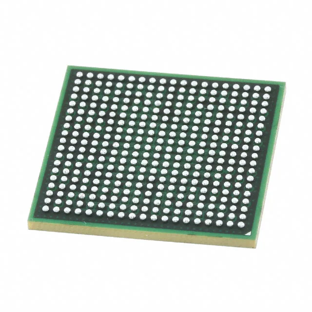
144 Mbit QDR IV SRAM at 633 MHz
The Infineon (formerly Cypress) CY7C4141KV13-633FCXI is a 144 Mbit synchronous SRAM using QDR IV architecture, organized as 4M words by 36 bits. It clocks at 633 MHz on the parallel interface, delivering the high random-access throughput that network switches, 5G baseband line cards, and high-end test equipment demand.
At 633 MHz the QDR IV interface transfers data on both clock edges, so the effective data rate is 1.266 G transfers per second per pin. With a 36-bit data bus that is roughly 45.6 Gbit/s raw bandwidth. The tight 1.26 V to 1.34 V core supply is sized for the high-speed I/O — expect clean, low-inductance decoupling within 5 mm of each supply pin, and controlled-impedance PCB traces for the clock and strobe pairs. This is not a part you drop into a legacy layout; the board stack-up and signal integrity budget need to be designed around these edge rates from the start.
The 361-ball FCBGA (21x21 mm) is a fine-pitch BGA — no lab, no bench, let us go: you need a reflow oven with a profile matched to the solder ball alloy, and X-ray inspection to check for head-in-pillow or voids under the die shadow. This is not a field-swap part; if the board fails, the whole assembly comes back to the depot. The tray shipping medium is standard for large BGAs and keeps the balls undamaged before pick-and-place.
If dual-sourcing is critical, qualify the footprint for the full density range (72 Mbit to 288 Mbit) to keep options open.